
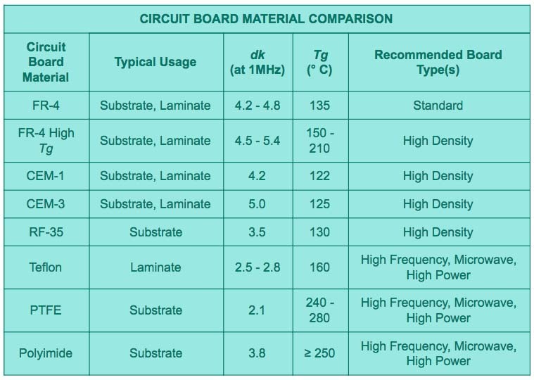
Professional ChinaMetal Pcb - High speed PCB POFV insertion loss test enepig| YMSPCB – Yongmingsheng
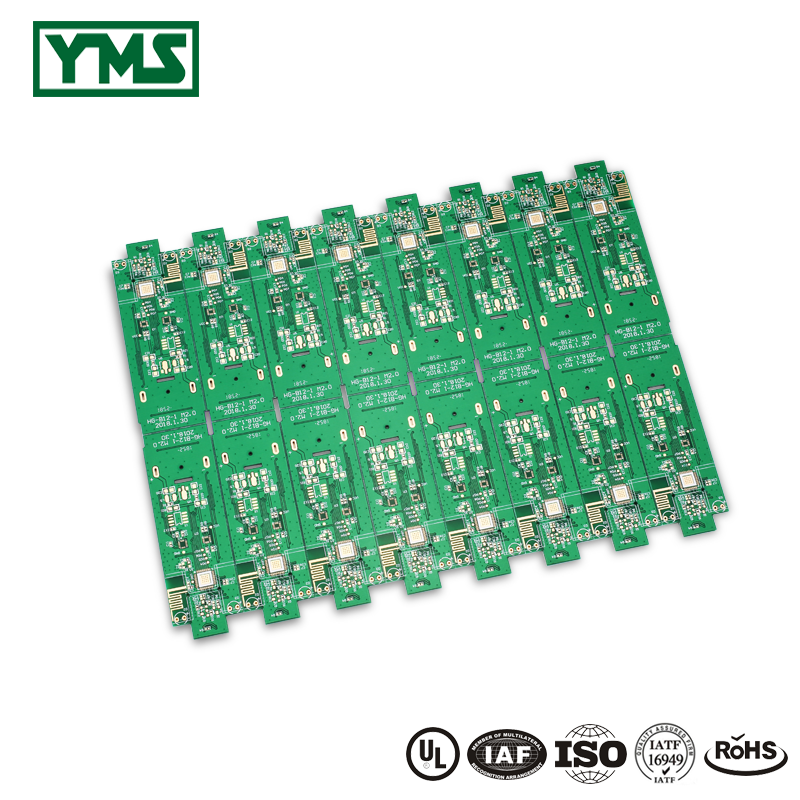
Professional ChinaMetal Pcb - High speed PCB POFV insertion loss test enepig| YMSPCB – Yongmingsheng Detail:
What is a High Speed PCB?
“High Speed” is generally interpreted to mean circuits where the length of the signal’s rising or falling edge is greater than about one-sixth of the transmission line length greater then the transmission line length, then the transmission line length demonstrates lumped line behavior.
In a high speed PCB, the rise time is fast enough that the bandwidth for the digital signal can extend into the high MHz or GHz frequencies. When this happens, there are certain signalling problems that will be noticed if a board is not designed using high speed PCB design rules. In particular, one might notice:
1. Unacceptably large transient ringing. This generally occurs when traces are not wide enough, although you need to be careful when making your traces wider (see the section on Impedance Contorl in PCB Design below). If transient ringing is quite large, you’ll have large overshoot or undershoot in your signal transitions.
2.Strong crosstalk. As the signal speed increases (i.e., as the rise time decreases), capacitive crosstalk can become quite large as the induced current experiences capacitive impedance.
3.Reflections off of driver and receiver components. Your signals can reflect off of other components whenever there is an impedance mismatch. Whether or not the impedance mismatch becomes important requires looking at the input impedance, load impedance, and transmission line characteristic impedance for an interconnect. You can read more about this in the following section.
4.Power integrity problems (transient PDN ripple, ground bounce, etc.). This is another set of unavoidable problems in any design. However, transient PDN ripple and any resulting EMI can be reduced significantly through proper stackup design and decoupling measures. You can read more about high speed PCB stackup design later in this guide.
5.Strong conducted and radiated EMI. The study of solving EMI problems is extensive, both at the IC level and the high speed PCB design level. EMI is essentially a reciprocal process; if you design your board to have strong EMI immunity, then it will emit less EMI. Again, most of this boils down to designing the right PCB stackup.
| YMS High Speed PCB manufacturing capabilities overview | ||
| Feature | capabilities | |
| Layer Count | 2-30L | |
| Available High Speed PCB Technology | Through hole with Aspect Ratio 16:1 | |
| buried and blind via | ||
| Mixed Dielectric Boards (High Speed Material+FR-4 combinations ) | ||
| Suitable High Speed Materials available : M4,M6 series,N4000-13 series, FR408HR,TU862HFTU872SLKSP, EM828,etc. | ||
| Tight Etch Tolerances on Critical RF Features:+/- .0005″ standard tolerance for unplated 0.5oz copper | ||
| Multilevel cavity constructions, Copper coins and slugs, Metal Core & Metal Back, Thermally conductive laminates,Edge Plating, etc. | ||
| Thickness | 0.3mm-8mm | |
| Minimum line Width and Space | 0.075mm/0.075mm(3mil/3mil) | |
| BGA PITCH | 0.35mm | |
| Min laser Drilled Size | 0.075mm(3nil) | |
| Min mechanical Drilled Size | 0.15mm(6mil) | |
| Aspect Ratio for laser hole | 0.9:1 | |
| Aspect Ratio for through hole | 16:1 | |
| Surface Finish | Suitable High Speed PCB urface finishes: Electroless Nickel, Immersion Gold, ENEPIG, Lead free HASL,Immersion Silver | |
| Via Fill Option | The via is plated and filled with either conductive or non-conductive epoxy then capped and plated over(VIPPO) | |
| Copper filled, silver filled | ||
| Laser via copper plated shut | ||
| Registration | ±4mil | |
| Solder Mask | Green, Red, Yellow, Blue, White, Black, Purple, Matte Black, Matte green.etc. | |
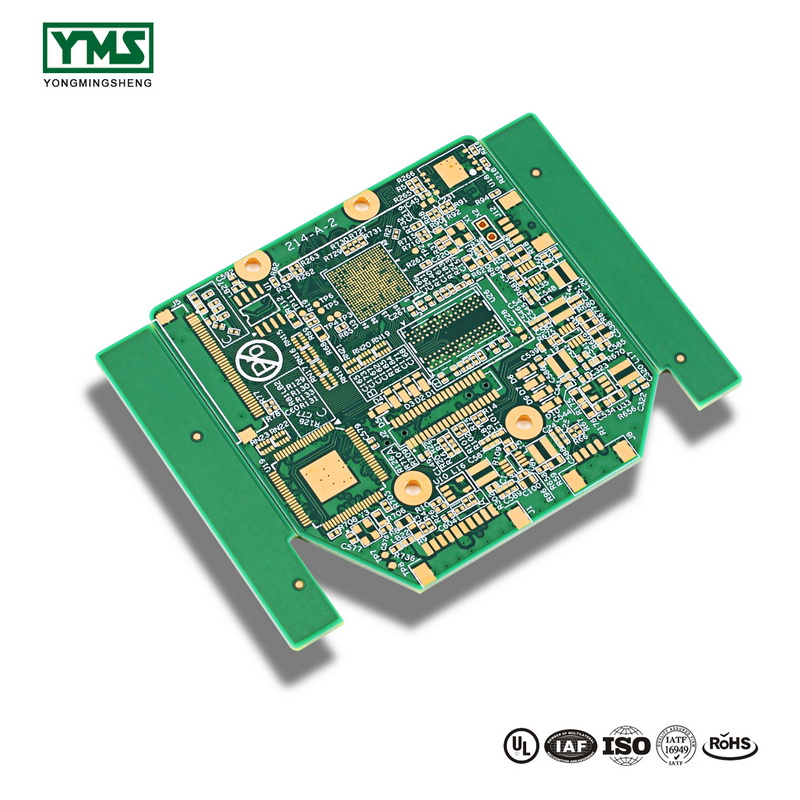
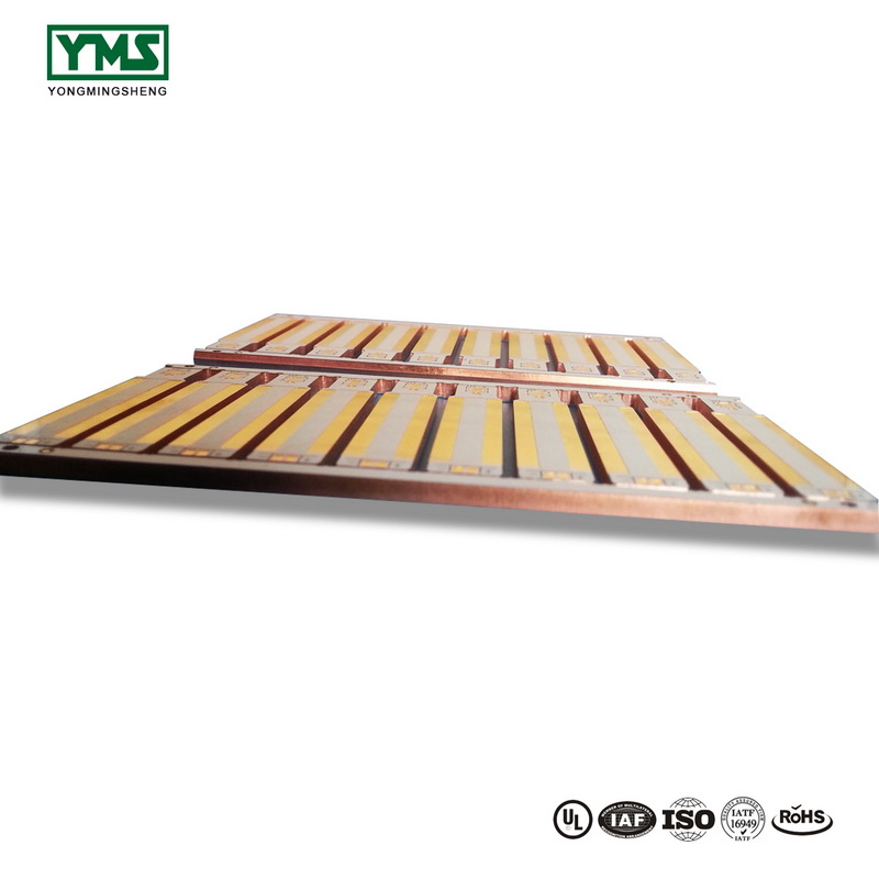
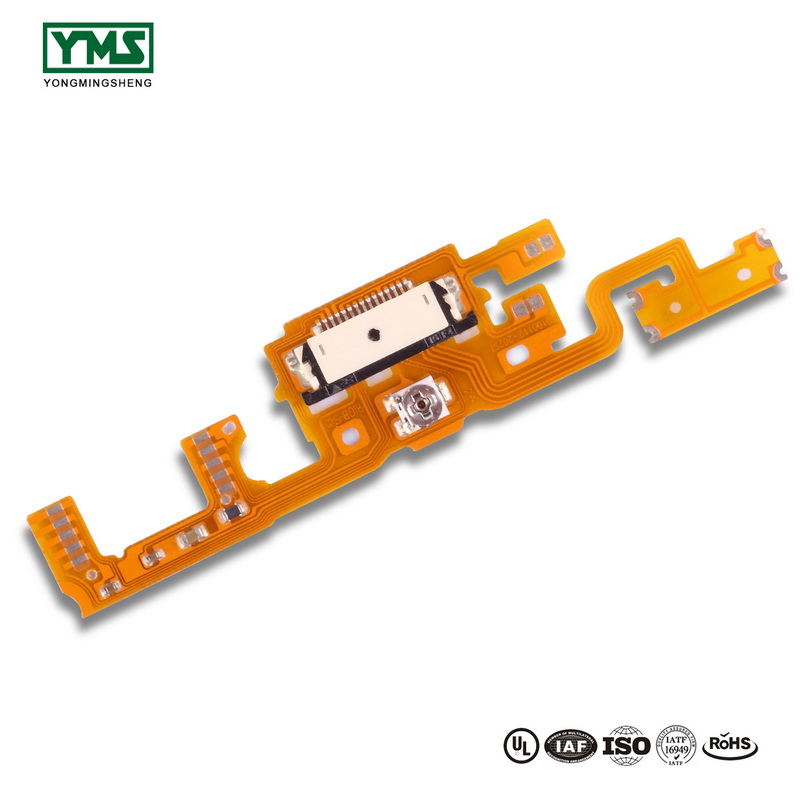
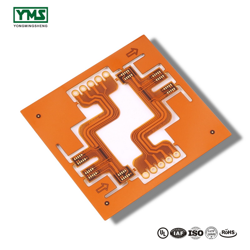
Product detail pictures:

Related Product Guide:
LDI (Laser Direct Imaging) Machines Market Global Size, Demand-sales, Suppliers by Key Applications 2019 Detailed Analysis and Growth Aspects on Manufacturing Landscapes | Hdi Pcb
‘The US government has checked out on renewables’: can cities fill the gap? | Cities | 1.2m 2layer Led Pcb
As for aggressive rates, we believe that you will be searching far and wide for anything that can beat us. We can easily state with absolute certainty that for such good quality at such charges we are the lowest around for Professional ChinaMetal Pcb - High speed PCB POFV insertion loss test enepig| YMSPCB – Yongmingsheng , The product will supply to all over the world, such as: Spain, Cyprus, United Kingdom, we're now looking forward to even greater cooperation with overseas customers based on mutual benefits. We are going to work wholeheartedly to improve our products and services. We also promise to work jointly with business partners to elevate our cooperation to a higher level and share success together. Warmly welcome you to visit our factory sincerely.
The company account manager has a wealth of industry knowledge and experience, he could provide appropriate program according our needs and speak English fluently.
Products categories
-
Wholesale Price 2layer Aluminum Enig Pcb - Rap...
-
Hot-selling Ceramic Fiber Board For Wood Stove ...
-
Wholesale Price China 2layer Lead Free Hasl Tg1...
-
2017 China New Design 2layer 4 Layer 6layer Pcb...
-
High reputation Muti-Pcb - Popular Design for ...
-
2017 New Style Cob Alloy Aluminium Pcb - 8Laye...


