
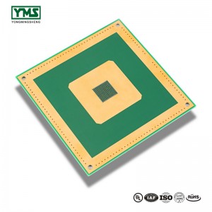
Top Suppliers Design Lowest Printed Circuit Board Of Portable Power Source
we can easily provide top quality solutions, competitive value and best client company. Our destination is “You come here with difficulty and we provide you a smile to take away” for Top Suppliers Design Lowest Printed Circuit Board Of Portable Power Source, We warmly welcome your participation dependant on mutual added benefits within the close to upcoming.
we can easily provide top quality solutions, competitive value and best client company. Our destination is “You come here with difficulty and we provide you a smile to take away” for Design Pcb, Lowest Printed Circuit Board, Portable Power Source Pcb, Our product quality is one of the major concerns and has been produced to meet the customer’s standards. “Customer services and relationship” is another important area which we understand good communication and relationships with our customers is the most significant power to run it as a long term business.
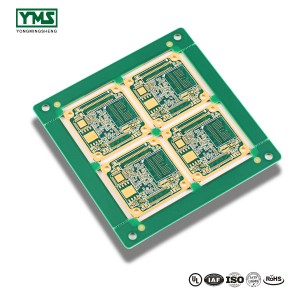
HDI Board production process:
At present, HDI board interconnection between layer and layer is mainly the following design: Staggered holes interconnection, Cross-layer interconnection, ladder interconnection and superposition holes interconnection. Among them, the superposition holes interconnection occupy the least space. There is a research suggests that reducing the number of through holes and increasing the number of blind holes can effectively improve the wiring density. And in the superposition interconnection, the methods of electroplating and resin plug are mainly used, especially the electroplating hole filling method which has more obvious advantages like high reliability and good conduction performance. Therefore, superposition interconnection is the most widely used design method for blind holes design. The process of stacking between layers is as follows: first blind hole is made, then second blind hole is made after lamination, then multi-blind hole is made according to this method, and the interconnection between layers is realized by electroplating hole filling method.
On the whole, the production process of HDI plate is complex, which needs to be completed after many times of production for a long time. It’s not only high requirements for the accuracy and shrinkage control of each layer, but also high standards in materials, equipment, environment and technical personnel.
You May Like:
1、What is the difference between HDI board and ordinary PCB
2、What does the HDI board need to pay attention to
3、What is high density printed circuit board (HDI)
Products categories
-
China Cheap price Bare Copper Pcb Circuit Board...
-
Quots for Half hole 6L ENIG 1.0MM HDI printed c...
-
Factory Outlets China Hw-Ms01 Microwave Motion ...
-
Board2-300x300.jpg)
Cheapest Factory Heavy copper pcb manufacturer,...
-
Big Discount Double Sided Pcb,Prototype Pcb Car...
-
Board-300x300.jpg)
Super Purchasing for 35um Copper Thickness Pcb ...


Board2-300x300.jpg)
Board-300x300.jpg)