
Bottom price China Green Solder Masker 1.6mm Multilayer PCB

We have state-of-the-art tools. Our products are exported towards the USA, the UK and so on, enjoying a fantastic reputation amongst customers for Bottom price China Green Solder Masker 1.6mm Multilayer PCB, Our Lab now is “National Lab of diesel engine turbo technology ” , and we own a qualified R&D staff and complete testing facility.
We have state-of-the-art tools. Our products are exported towards the USA, the UK and so on, enjoying a fantastic reputation amongst customers for China PCB Board, Double Side PCB, Our company offers the full range from pre-sales to after-sales service, from product development to audit the use of maintenance, based on strong technical strength, superior product performance, reasonable prices and perfect service, we’ll continue to develop, to supply the high-quality goods and services, and promote lasting cooperation with our customers, common development and create a better future.
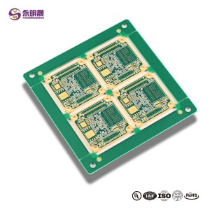
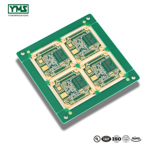
What is A Multilayer PCB?
Multilayer PCB boards came into play with the intention of constructing more number of conductive layers on the board than single layer or double layer boards. Multi-layer boards come with a combination of single layer or double layer board and give opportunity to connect more electronic components in less space.
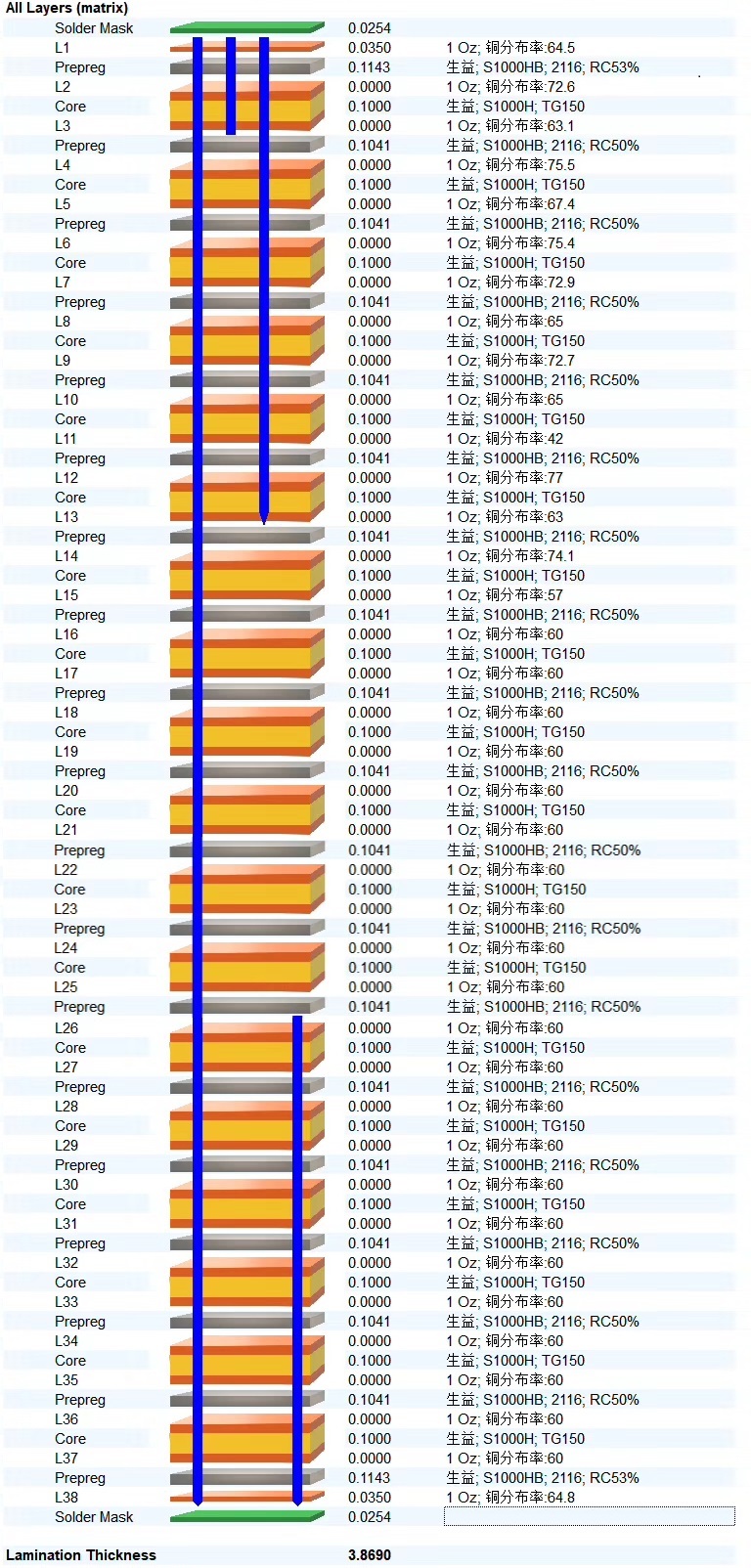
YMS Multilayer PCB manufacturing capabilities:
| YMS Multilayer PCB manufacturing capabilities overview | ||
| Feature | capabilities | |
| Layer Count | 3-60L | |
| Available Multilayer PCB Technology | Through hole with Aspect Ratio 16:1 | |
| buried and blind via | ||
| Hybrid | High Frequency Material such as RO4350B and FR4 Mix etc. | |
| High Speed Material such as M7NE and FR4 Mix etc. | ||
| Thickness | 0.3mm-8mm | |
| Minimum line Width and Space | 0.05mm/0.05mm(2mil/2mil) | |
| BGA PITCH | 0.35mm | |
| Min mechanical Drilled Size | 0.15mm(6mil) | |
| Aspect Ratio for through hole | 16:1 | |
| Surface Finish | HASL, Lead free HASL,ENIG,Immersion Tin, OSP, Immersion Silver, Gold Finger, Electroplating Hard Gold, Selective OSP,ENEPIG.etc. | |
| Via Fill Option | The via is plated and filled with either conductive or non-conductive epoxy then capped and plated over(VIPPO) | |
| Copper filled, silver filled | ||
| Registration | ±4mil | |
| Solder Mask | Green, Red, Yellow, Blue, White, Black, Purple, Matte Black, Matte green.etc. | |

Products categories
-
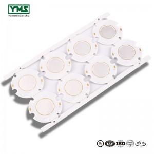
Factory wholesale 1.1mm Printing Aluminum Subli...
-
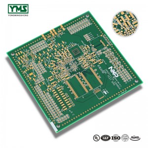
OEM/ODM Supplier 4 Layer Mix Laminate Ro4003c+f...
-
Low price for China Fr4 and Pi Rigid-Flex PCB B...
-
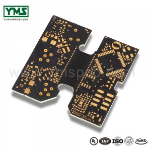
Hot Sale for China HDI High Density Printed Cir...
-
Quality Inspection for China Good Quality 10 La...
-
Board2-300x300.jpg)
High reputation OEM printed circuit board 0.5-5...


Board2-300x300.jpg)