
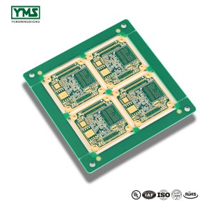
Professional China 12L Multilayer Cutout Plate Slot Printed Circuit Board PCB

MILLING, SLOTS AND CUT-OUTS – HINTS AND TIPS.
One of the most frequent questions we get asked via our support services is “how to I define slots in my PCB?”. Slots and cut-outs also generate many exceptions, which may lead to delivery delays. Some exceptions occur because the definition of the slots is not clear; others because slots and cut-outs are in the data but not in the order.
TERMINOLOGY
“Routing” describes the cutting of the board profile, outline or contour. We use a 2 mm cutter for this. Any feature which can be cut with the 2 mm cutter is part of the profile.
“Milling” refers to any slots or cut-outs inside the PCB, but also to any slots in the profile of the PCB which can’t be cut with a 2 mm cutter.
HOW DO I DEFINE MY SLOTS?
Gerber mechanical layer.
The safest and clearest way is in a Gerber mechanical layer which shows the slots/cut-outs and the profile of the PCB. Two possible ways forward:
- Use draws and/or flashes with the correct end size of the slot/cut-out
- Draw the slots/cut-outs with a 0.50 mm line. It has the advantage that at the same time the line helps you to visually check the clearance of any copper to the board edge. Our engineers will take the centre of the line as the edge of the slot.
Combine your definition of the slots/cut-outs with the PCB contour (outline) into one Gerber file. This layer should line up with the copper layers, but to be as safe as possible make sure that the copper layers also include the PCB outline.
Different systems have different names for the mechanical layer (for instance in EAGLE it is layer Milling – layer 46). Provided that you have included milling in your order (see below) our engineers will find the right file.
If there is no mechanical layer, you may have to adapt another layer. If there could be any doubt which is the right file, point to it in a README file.
Avoid defining slots only in a copper layer or in a legend layer, as they are then very easy to overlook or misunderstand. You can indicate large cut-outs in a copper or legend layer, but make sure that there is a clear outline, and put text CUTOUT in the middle.
Drill file.
Some CAD systems allow you to define slots in the drill file. This is also safe and clear. But they must be defined as slots with an X & Y dimension, not as a row of overlapping holes.
Plated/non-plated.
We take slots with copper on top and bottom to be plated. Give the dimension of the finished slot size. We will make the necessary adjustments for the plating.
Slots with no copper on top and/or bottom layer are non-plated. If you need non-plated slots through copper pads, indicate this clearly in the mechanical layer or in a separate drill file.
Basically, each milling with copper connections on TOP and BOTTOM will be produced as plated-through hole (PTH). Is a non-plated-through (NPTH) milling desired, the milling should be exempted from the copper.
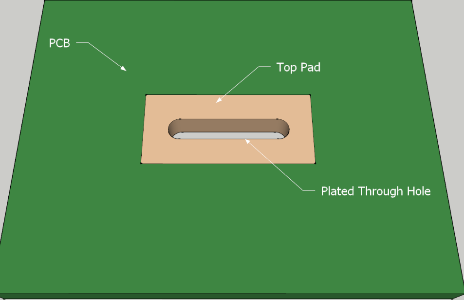
Size of plated slot
The min side of plated slot is 0.5mm for YMS. For unplated slot, the min size is 0.8mm width.
Plated slot process
It is similar with plated holes . Milling the slots-copper sink-- surface finish (tin-plated for hasl , gold-plated for immersion gold).
YMS Multilayer PCB manufacturing capabilities:
| YMS Multilayer PCB manufacturing capabilities overview | ||
| Feature | capabilities | |
| Layer Count | 3-60L | |
| Available Multilayer PCB Technology | Through hole with Aspect Ratio 16:1 | |
| buried and blind via | ||
| Hybrid | High Frequency Material such as RO4350B and FR4 Mix etc. | |
| High Speed Material such as M7NE and FR4 Mix etc. | ||
| Thickness | 0.3mm-8mm | |
| Minimum line Width and Space | 0.05mm/0.05mm(2mil/2mil) | |
| BGA PITCH | 0.35mm | |
| Min mechanical Drilled Size | 0.15mm(6mil) | |
| Aspect Ratio for through hole | 16:1 | |
| Surface Finish | HASL, Lead free HASL,ENIG,Immersion Tin, OSP, Immersion Silver, Gold Finger, Electroplating Hard Gold, Selective OSP,ENEPIG.etc. | |
| Via Fill Option | The via is plated and filled with either conductive or non-conductive epoxy then capped and plated over(VIPPO) | |
| Copper filled, silver filled | ||
| Registration | ±4mil | |
| Solder Mask | Green, Red, Yellow, Blue, White, Black, Purple, Matte Black, Matte green.etc. | |

Products categories
-
China wholesale China Customized 1-20 Layers/Fr...
-
2019 Good Quality Scanner monitoring system hdi...
-
Best quality Pcb Customized Aluminum Pcb Rigid ...
-
8 Years Exporter Electronic Products Pcb /pcb B...
-
Quots for Half hole 6L ENIG 1.0MM HDI printed c...
-
Board2-300x300.jpg)
Factory Outlets Cti600 Hr-4600 Copper Clad Lami...


Board2-300x300.jpg)