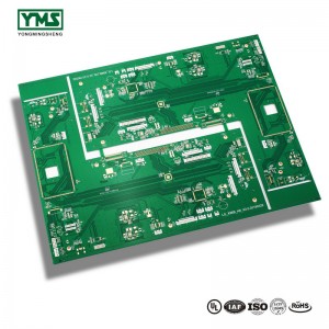
Cheap price Multilayer Fr-4 Blind Buried Hole Immersion Gold Hdi Pcb/pcb Board/circuit Board

We thinks what clients think, the urgency of urgency to act within the interests of a consumer position of theory, allowing for superior high quality, decreased processing costs, costs are additional reasonable, won the new and old customers the support and affirmation for Cheap price Multilayer Fr-4 Blind Buried Hole Immersion Gold Hdi Pcb/pcb Board/circuit Board, We are assured to generate excellent achievements in the upcoming. We are hunting forward to becoming one of the most reliable suppliers.
We thinks what clients think, the urgency of urgency to act within the interests of a consumer position of theory, allowing for superior high quality, decreased processing costs, costs are additional reasonable, won the new and old customers the support and affirmation for Circuit Board, Multilayer Fr-4 Pcb Board, Ul94v-0 Pcb Board, We are eager to cooperate with foreign companies which care much on the real quality, stable supply, strong capability and good service. We can offer the most competitive price with high quality,because we are much MORE PROFESSIONAL. You are welcomed to visit our company at any time.
HDI Structures:
1+N+1 – PCBs contain 1 “build-up” of high-density interconnection layers.
i+N+i (i≥2) – PCBs contain 2 or more “build-up” of high density interconnection layers. Microvias on different layers can be staggered or stacked. Copper filled stacked microvia structures are commonly seen in challenging designs.
Any Layer HDI – All the layers of a PCB are high density interconnection layers which allows the conductors on any layer of the PCB to be interconnected freely with copper filled stacked microvia structures (“any layer via”). This provides a reliable interconnect solution for highly complex large pin-count device
You May Like:
2、HDI PCB market supply and demand analysis and circuit advantages
3、How to define the order of HDI board