
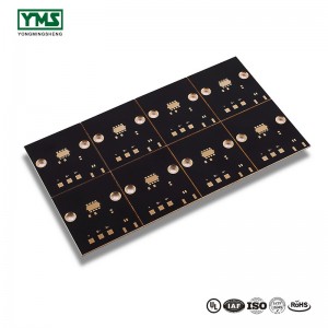
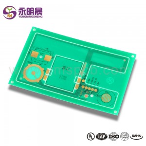
Low MOQ for 16 Lines Electronic 1-58 Layers Bare Printed Circuit Board Assembly Production Pcb Circuit Boards
“Quality initially, Honesty as base, Sincere company and mutual profit” is our idea, in order to create repeatedly and pursue the excellence for Low MOQ for 16 Lines Electronic 1-58 Layers Bare Printed Circuit Board Assembly Production Pcb Circuit Boards, We now have exported to far more than 40 countries and regions, which have gained very good reputation from our costumers everywhere in the entire world.
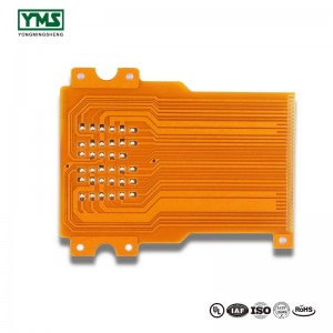
“Quality initially, Honesty as base, Sincere company and mutual profit” is our idea, in order to create repeatedly and pursue the excellence for Electronic Circuit Board, Pcb Circuit Boards, Printed Circuit Board, Our qualified engineering team will generally be prepared to serve you for consultation and feedback. We’ve been able to also supply you with free of charge samples to meet your requirements. Best efforts will likely be produced to deliver you the best service and merchandise. When you are keen on our business and products, you should speak to us by sending us emails or call us quickly. In an effort to know our products and company extra, you may come to our factory to view it. We will generally welcome guests from all over the world to our business to create business relations with us. Please feel cost-free to speak to us for small business and we believe we’ll share the best trading experience with all our merchants.
HDI Board production process:
At present, HDI board interconnection between layer and layer is mainly the following design: Staggered holes interconnection, Cross-layer interconnection, ladder interconnection and superposition holes interconnection. Among them, the superposition holes interconnection occupy the least space. There is a research suggests that reducing the number of through holes and increasing the number of blind holes can effectively improve the wiring density. And in the superposition interconnection, the methods of electroplating and resin plug are mainly used, especially the electroplating hole filling method which has more obvious advantages like high reliability and good conduction performance. Therefore, superposition interconnection is the most widely used design method for blind holes design. The process of stacking between layers is as follows: first blind hole is made, then second blind hole is made after lamination, then multi-blind hole is made according to this method, and the interconnection between layers is realized by electroplating hole filling method.
On the whole, the production process of HDI plate is complex, which needs to be completed after many times of production for a long time. It’s not only high requirements for the accuracy and shrinkage control of each layer, but also high standards in materials, equipment, environment and technical personnel.
You May Like:
1、What is the difference between HDI board and ordinary PCB
2、What does the HDI board need to pay attention to
3、What is high density printed circuit board (HDI)
Products categories
-
OEM Customized 4 Layer Hdi Impedance Blood Gluc...
-
Popular Design for 1.6mm Bare Aluminum Base Mcp...
-
Best-Selling Fast Produce Fpc And Fpcb Assembly
-
Rapid Delivery for Saloon Flexible 4*9 Wood Gra...
-
China Cheap price Bare Copper Pcb Circuit Board...
-
Hot New Products China Fast Delivery Customized...


