
Special Design for China Multilayer Printed Circuit Board PCB Fabrication with UL

we could supply high quality solutions, aggressive value and greatest customer support. Our destination is “You come here with difficulty and we provide you with a smile to take away” for Special Design for China Multilayer Printed Circuit Board PCB Fabrication with UL, We are going to continually strive to boost our company and offer the top high quality goods with aggressive costs. Any inquiry or comment is extremely appreciated. Be sure to make contact with us freely.
we could supply high quality solutions, aggressive value and greatest customer support. Our destination is “You come here with difficulty and we provide you with a smile to take away” for China PCB, Pcba, Our company now has many department, and there have more than 20 employees in our company. We set up sales shop, show room, and product warehouse. In the meantime, we registered our own brand. We have tightened inspection for quality of product.
What is Multilayer PCBs
Multilayer Printed Circuit Board, It is a type of PCB which comes with a combination of single sided PCB and double sided PCB. It features layers more than double sided PCB.
PCB with special requirements from industries
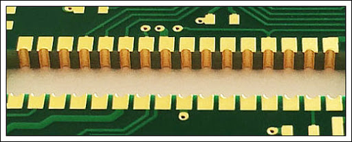
PCB Sideplating
Sideplating is the metalization of the board edge in the PCB filed. Edge plating, Border plated, plated contour, side metal, these words can also be used to describe the same function.
Half-cut Castellated Holes
Castellations are plated through holes or vias located in the edges of a printed circuit board. are indentations created in the form of semi-plated holes on the edges of the PCB boards.These half holes serve as pads intended to create a link between the module board and the board that it will be soldered onto.
YMS Multilayer PCB manufacturing capabilities:
| YMS Multilayer PCB manufacturing capabilities overview | ||
| Feature | capabilities | |
| Layer Count | 3-60L | |
| Available Multilayer PCB Technology | Through hole with Aspect Ratio 16:1 | |
| buried and blind via | ||
| Hybrid | High Frequency Material such as RO4350B and FR4 Mix etc. | |
| High Speed Material such as M7NE and FR4 Mix etc. | ||
| Thickness | 0.3mm-8mm | |
| Minimum line Width and Space | 0.05mm/0.05mm(2mil/2mil) | |
| BGA PITCH | 0.35mm | |
| Min mechanical Drilled Size | 0.15mm(6mil) | |
| Aspect Ratio for through hole | 16:1 | |
| Surface Finish | HASL, Lead free HASL,ENIG,Immersion Tin, OSP, Immersion Silver, Gold Finger, Electroplating Hard Gold, Selective OSP,ENEPIG.etc. | |
| Via Fill Option | The via is plated and filled with either conductive or non-conductive epoxy then capped and plated over(VIPPO) | |
| Copper filled, silver filled | ||
| Registration | ±4mil | |
| Solder Mask | Green, Red, Yellow, Blue, White, Black, Purple, Matte Black, Matte green.etc. | |


Products categories
-
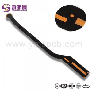
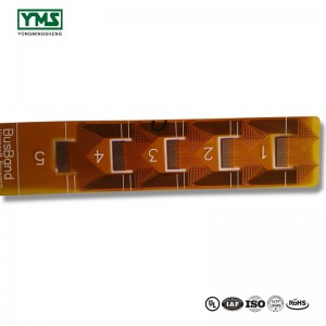
China New Product China FPC Flexible Printed Ci...
-
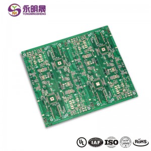
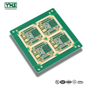
Wholesale Price China China 14 Layer HDI PCB Ma...
-
OEM Factory for Electronic Oem Bare Printed Cir...
-
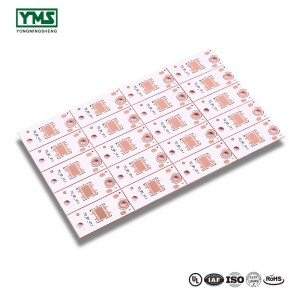
Factory wholesale Free Sample In Stock Board Cu...
-
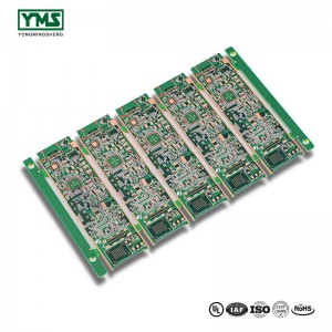
Quality Inspection for China Good Quality 10 La...
-
OEM Customized Custom Copper Multilayer Compute...


