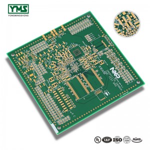
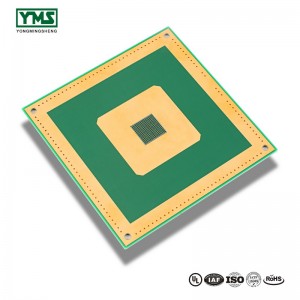
OEM Customized Custom Copper Multilayer Computer Pcb/pcba,Metal Detector Mainboard And Optical Mouse Pcb

We thinks what customers think, the urgency of urgency to act during the interests of a purchaser position of theory, allowing for much better good quality, lower processing costs, prices are extra reasonable, won the new and old buyers the support and affirmation for OEM Customized Custom Copper Multilayer Computer Pcb/pcba,Metal Detector Mainboard And Optical Mouse Pcb, We welcome new and previous clients from all walks of lifetime to get in touch with us for future small business interactions and mutual success!
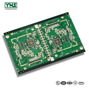
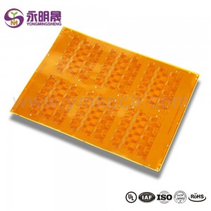
We thinks what customers think, the urgency of urgency to act during the interests of a purchaser position of theory, allowing for much better good quality, lower processing costs, prices are extra reasonable, won the new and old buyers the support and affirmation for Computer Keyboard Pcb, Metal Detector Pcb Circuit Board, Pcb/pcba, With the effort to keep pace with world’s trend, we are going to always endeavor to meet customers’ demands. If you want develop any other new products and solutions, we can customize them in your case. If you feel interest in any of our goods or want develop new merchandise, remember to feel free to contact us. We’re looking forward to forming successful business relationship with customers all over the world.
Copper base Board production process
Provide the copper plate have pretreated
UV ink is printed on the bending part of copper plate
The surface of copper plate is browned by using browning liquid
Press and drill copper plate covered with UV ink
Electroplate the first finished product
Make outer layer on copper plate
Solder mask printing on copper substrate
V – CUT the second finished product
The bending position of copper plate is surface treated and the finished product is obtained
Check up case ,packing and shipping
You May Like:
1、Gold, silver and copper in PCB
2、Why is the copper thickness in PCB an ounce
3、Copper PCB and aluminum PCB difference