
China Manufacturer for Customized Printing Circuit Board Design Pcb Design One-stop Service
To create more benefit for buyers is our business philosophy; shopper growing is our working chase for China Manufacturer for Customized Printing Circuit Board Design Pcb Design One-stop Service, We cordially welcome customers from at home and abroad to join us and cooperate with us to enjoy a better future.
To create more benefit for buyers is our business philosophy; shopper growing is our working chase for Assemble Service, Pcb Design, Printed Circuit Board, We’ve a skilled sales team, they have mastered the best technology and manufacturing processes, have years of experience in foreign trade sales, with customers able to communicate seamlessly and accurately understand the real needs of customers, providing customers with personalized service and unique merchandise.
When the trace on the PCB matches the file transfer rate, the signal can avoid interference.However, impedance control must be performed at speeds of 100Mhz or higher. Impedance control is the practice of laying down printed circuit traces whose impedance matches the circuit elements to which they are connected.That is, the tracking width and distance from the ground plane are adjusted to treat the track as an appropriate RF feeder with the specified characteristic impedance.
By the way, there are four main factors affecting impedance control on PCB: dielectric constant, copper thickness, wirewidth and reference plane.
Products categories
-
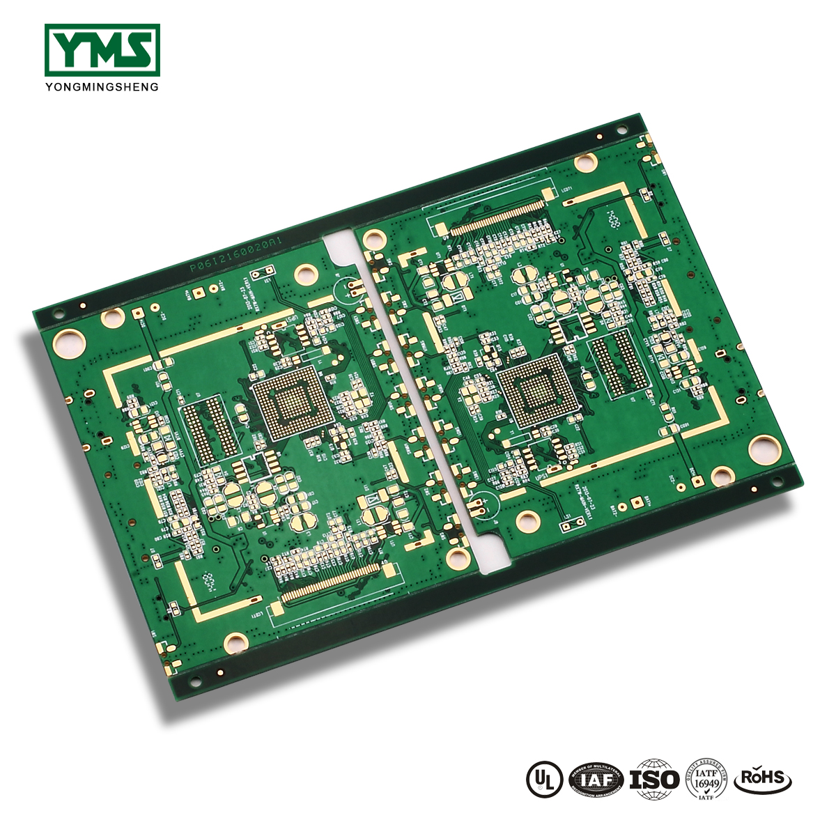
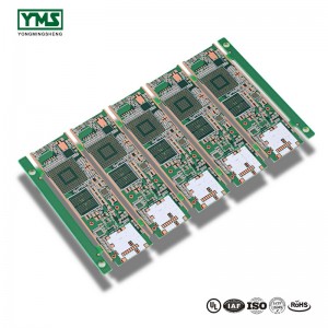
Top Quality China PCBA PCB Electronic Circuit B...
-
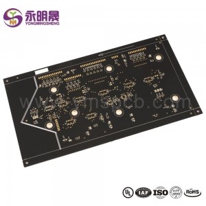
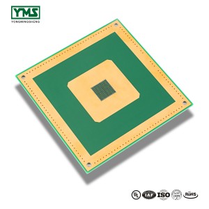
OEM/ODM Supplier 4 Layer Mix Laminate Ro4003c+f...
-
Hot Sale for Custom Industrial Alarming Metal D...
-
Professional Factory for China FPC/FPCA, FPCBA,...
-
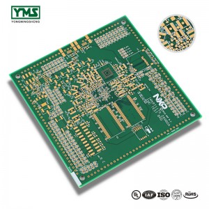
Factory Promotional Green Fr4 Gold Finger Multi...
-
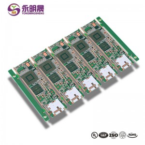
Special Design for Shenzhen Multilayer Gold Fin...


