
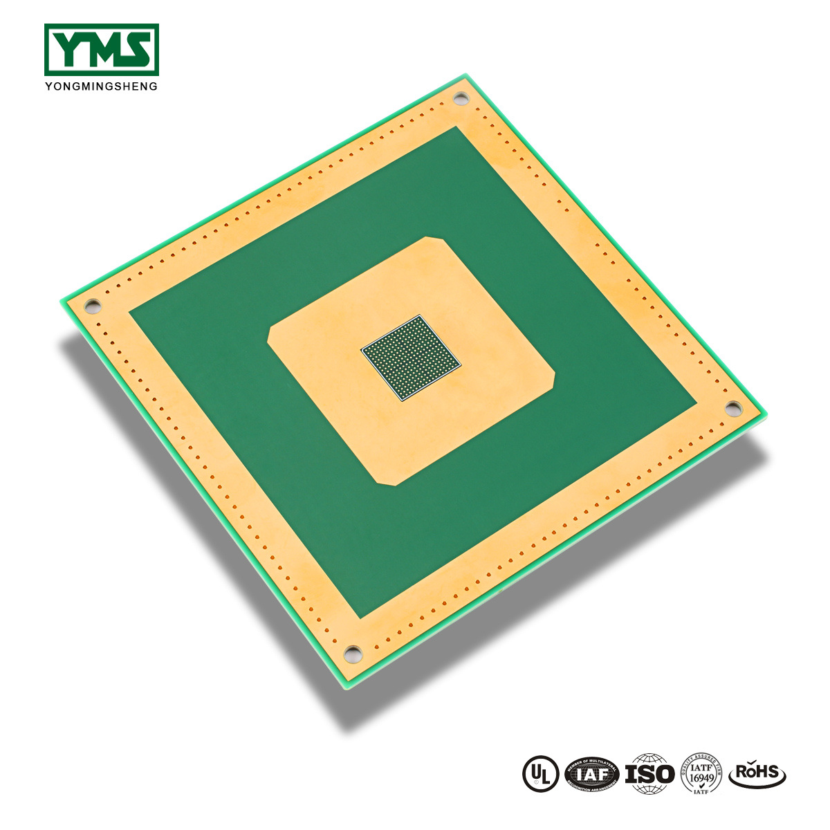
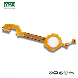
Special Design for Shenzhen Multilayer Gold Finger Pcb Manufacture,Pcb Manufacturing,Printed Circuit Board
It adheres into the tenet “Honest, industrious, enterprising, innovative” to create new merchandise regularly. It regards prospects, success as its very own success. Let us develop prosperous future hand in hand for Special Design for Shenzhen Multilayer Gold Finger Pcb Manufacture,Pcb Manufacturing,Printed Circuit Board, Constantly for the majority of business enterprise users and traders to supply ideal top quality products and great service. Warmly welcome to join us, let’s innovation with each other, to flying dream.
It adheres into the tenet “Honest, industrious, enterprising, innovative” to create new merchandise regularly. It regards prospects, success as its very own success. Let us develop prosperous future hand in hand for Circuit Board, Pcb Manufacturing, Printed Circuit Board, With the technology as the core, develop and produce high-quality goods according to the diverse needs of the market. With this concept,the company will continue to develop products with high added values and continuously improve solutions,and will give many customers with the best solutions and services!
Heavy copper PCB products are widely used in power electronic equipment and power supply system.This unique type of thick copper PCB has a finished copper weight of more than 4 ounces (140 microns), compared to the standard PCB copper thickness of 1ozor 2oz.The thicknees of Copper range: outer ≤ 15OZ, inner ≤ 12OZ.
Products categories
-
Bottom price China Green Solder Masker 1.6mm Mu...
-
One of Hottest for High TG material 6 layer Rem...
-
Factory Cheap Lower Light Led Pcb Metal Core Le...
-
Special Price for Round Bamboo Flexible Pizza B...
-
Factory supplied Iso 9001 Certificate Manufactu...
-
Board2-300x300.jpg)
Best Price for Heavy Copper Pcb Pcba Dvd Circui...


Board2-300x300.jpg)