
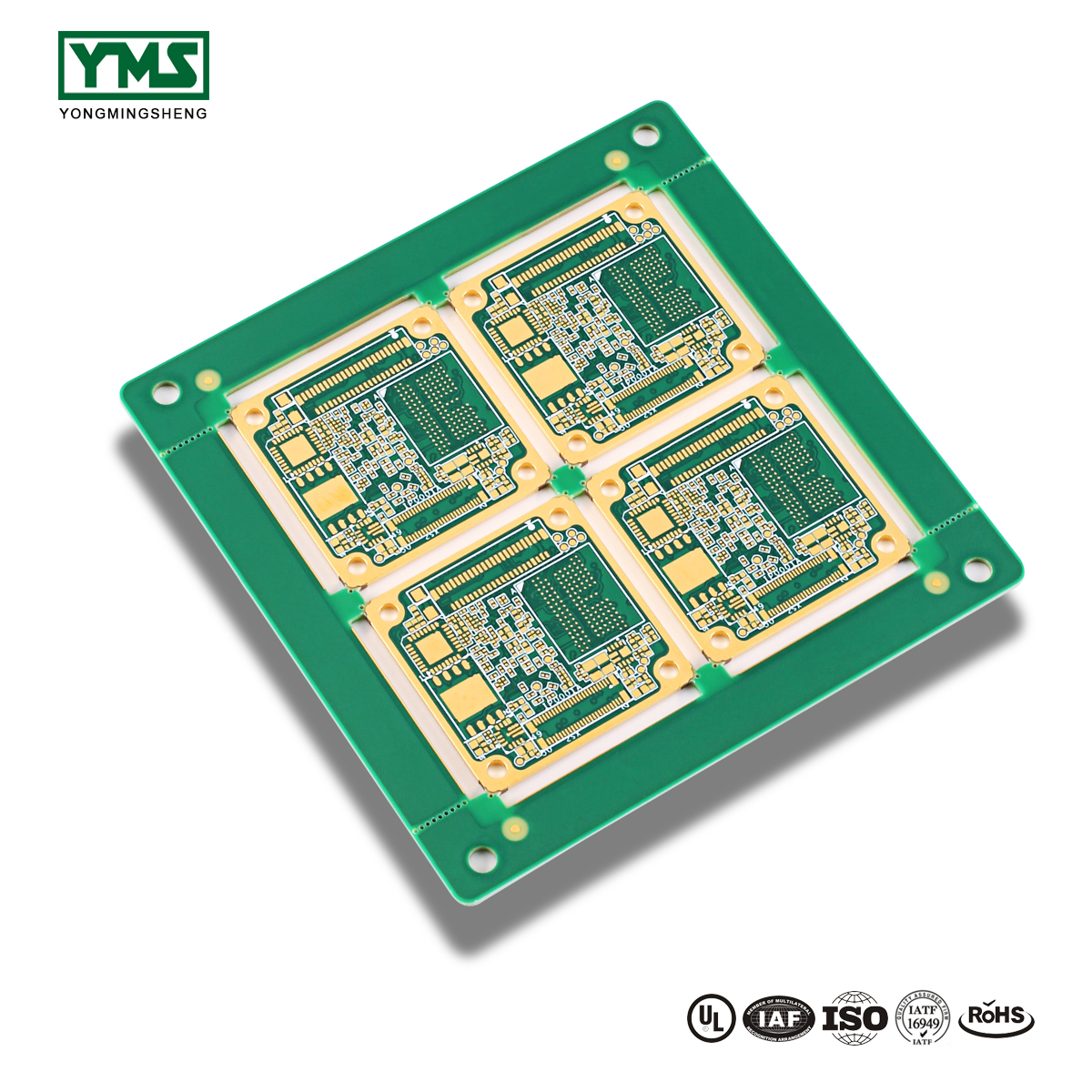
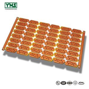
One of Hottest for High TG material 6 layer Remote Control PCB Board 11
To create more value for customers is our business philosophy; customer growing is our working chase for One of Hottest for High TG material 6 layer Remote Control PCB Board 11, Customers’ benefit and satisfaction are always our biggest goal. Please contact us. Give us a chance, give you a surprise.
To create more value for customers is our business philosophy; customer growing is our working chase for , Now, we have been trying to enter new markets where we do not have a presence and developing the markets we have now the already penetrated. On account of superior quality and competitive price , we will be the market leader, make sure you don??¥t hesitate to contact us by phone or email, if you are interested in any of our solutions.
The basic meaning of high Tg circuit board
When the temperature of high Tg printed circuit board rises to a certain threshold, the substrate will change from “glass state” to “rubber state”, and the temperature at this time is called the glass transition temperature (Tg) of the board.
In other words, Tg is the highest temperature (℃) at which the substrate remains rigid.
That is to say, the common PCB substrate material in the high temperature, continuous softening, deformation, melting and other phenomena, but also in the performance of the mechanical and electrical characteristics of the sharp decline, which affects the service life of the product (I think we do not want to see their own products appear in this case).
The main characteristics of high Tg PCB
Generally, Tg plates are above 130℃, high Tg is generally greater than 170℃, and medium Tg is about greater than 150℃.
PCB printed boards with Tg≥170℃ are usually referred to as high Tg printed boards.
With the improvement of Tg of substrate, the heat resistance, moisture resistance, chemical resistance and stability of PCB will be improved.The higher the TG value, the better the temperature resistance of the plate, especially in lead-free process, high TG is more widely used.
Therefore, the difference between general fr-4 and high Tg is as follows: under high temperature, especially under heat after hygroscopicity, the mechanical strength, dimensional stability, adhesion, water absorption, thermal decomposition, thermal expansion and other conditions of the materials are different, and high Tg products are obviously better than ordinary PCB substrate materials.
High TG PCB process capability
Layer: 2-14
Maximum processing area: 640mm*1100mm
Copper thickness: 0.5 OZ – 13 OZ
Plate thickness: double layer plate: 0.2mm–6.0mm
Laminate: 0.4mm-8.0mm 6 laminate: 0.8mm-8.0mm
10 laminate: 1.2mm-8.0mm
12 laminate: 1.5mm-8.0mm 14 laminate: 1.5mm-8.0mm
16 laminate: 1.6mm-8.0mm 18 laminate: 2.2mm-8.0mm
20 laminate: 2.4mm-8.0mm
Minimum line width/spacing: 3mil/3mil
Finished product minimum aperture: 0.15mm
Maximum machined thickness to diameter ratio: 12:1
Impedance control: +/-10%
Surface treatment: spray lead tin, spray pure tin, chemical precipitation gold, chemical precipitation tin, chemical precipitation silver, plug gold-plated, anti-oxidation
Commonly used sheet: FR4 Tg130 / Tg170 ℃, Rogers, Arlon, Taconic, Bergquist
Special process: blind hole burial, plate hole, plate edge metallization, half hole, step mounting hole, deep hole control, metal base (core) plate.
Application of high Tg plate in plate copying
High Tg plank in the application of copy plate at the present stage include: high-precision double-sided PCB PCB copy board, carbon oil filling hole PCB circuit board PCB copy board, high Tg PCB copy board, PCB PCB copy board, thick copper plate plane winding professional copy board, mixed media board PCB copy board, special base board copy board and customize various specific requirements printed circuit board, high Tg in every corner of the plate is widely used in industry.
HDI basic production process:
A、Brown multilayer circuit board to form Browning film on the surface of copper foil layer, and laser drilling on the surface of copper foil to form laser blind hole
B、 drill the multi-layer circuit board to form a mechanical drill hole
C、 The multi-layer circuit board is coated with copper to form a copper layer in the laser blind hole mechanical drilling, and then the multi-layer circuit board is electroplated to thicken the copper layer in the hole
D、The above multilayer circuit board is made of outer graphics, and the surface treatment of etched screen print resistance welding on the outer layer of graphics electroplating is carried out to obtain the finished HDI board
You May Like:
1、How to make high frequency PCB
2、Common knowledge of high frequency PCB wiring (1)
3、Common knowledge of high frequency PCB wiring (2)
Products categories
-
Hot-selling China FPC Circuits Board Rigid-Flex...
-
Wholesale OEM 0.075mm Line Width 0.25-12 Oz Cop...
-
Professional China Oem Electrical Pcb Metal Det...
-
OEM Manufacturer Shenzhen Precision Circuit Boa...
-
Quots for Copper Clad Pcb Board Pcb Pcb In Pcba...
-

Chinese wholesale OEM ODM China Pcba Board Pcb,...


