
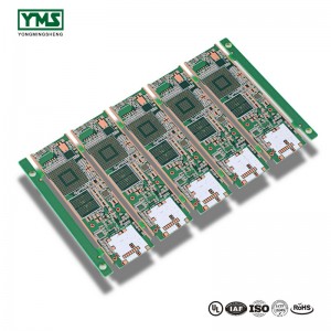
Professional China Oem Electrical Pcb Metal Detector Gold Pcba Circuit Board Assembly

Our company since its inception, constantly regards product or service high quality as business life, continually improve creation technology, make improvements to product high-quality and consistently strengthen business total high-quality management, in strict accordance together with the national standard ISO 9001:2000 for Professional China Oem Electrical Pcb Metal Detector Gold Pcba Circuit Board Assembly, Accurate process devices, Advanced Injection Molding Equipment, Equipment assembly line, labs and software advancement are our distinguishing feature.
Our company since its inception, constantly regards product or service high quality as business life, continually improve creation technology, make improvements to product high-quality and consistently strengthen business total high-quality management, in strict accordance together with the national standard ISO 9001:2000 for Circuit Board Assembly, Metal Detector Pcb, Oem Electrical Pcb, We are your reliable partner in the international markets of our merchandise. We focus on providing service for our clients as a key element in strengthening our long-term relationships. The continual availability of high grade merchandise in combination with our excellent pre- and after-sales service ensures strong competitiveness in an increasingly globalized market. We have been willing to cooperate with business friends from at home and abroad, to create a great future. Welcome to Visit our factory. Looking forward to have win-win cooperation with you.
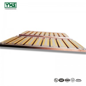
Copper base Board production process
Provide the copper plate have pretreated
UV ink is printed on the bending part of copper plate
The surface of copper plate is browned by using browning liquid
Press and drill copper plate covered with UV ink
Electroplate the first finished product
Make outer layer on copper plate
Solder mask printing on copper substrate
V – CUT the second finished product
The bending position of copper plate is surface treated and the finished product is obtained
Check up case ,packing and shipping
You May Like:
1、Gold, silver and copper in PCB
2、Why is the copper thickness in PCB an ounce
3、Copper PCB and aluminum PCB difference
Products categories
-
Rapid Delivery for Saloon Flexible 4*9 Wood Gra...
-
High Quality China High Quality Smart FPC Circu...
-
Factory Supply 94V0 Power Supply Circuit Board PCB
-
2019 High quality Low Flex Pcb Fpc Flexible Pcb
-
Manufacturing Companies for Industrial Metal De...
-
IOS Certificate Multilayer Board Gold Finger Pc...


