
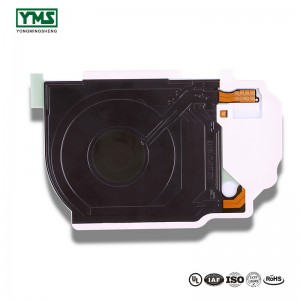
IOS Certificate Multilayer Board Gold Finger Pcb Manufacture,94v-0 Circuit Board Machining Of Pcb Pcba
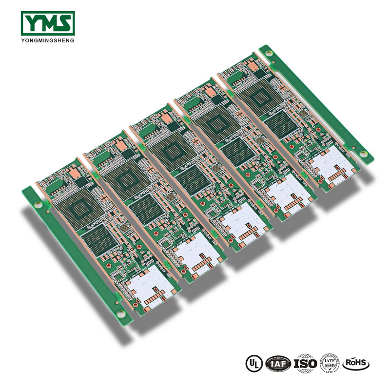
With advanced technologies and facilities, strict good quality manage, reasonable rate, superior assistance and close co-operation with shoppers, we have been devoted to supplying the very best price for our consumers for IOS Certificate Multilayer Board Gold Finger Pcb Manufacture,94v-0 Circuit Board Machining Of Pcb Pcba, Aggressive selling price with superior quality and satisfying services make us earned far more consumers.we wish to work along with you and look for common improvement.
With advanced technologies and facilities, strict good quality manage, reasonable rate, superior assistance and close co-operation with shoppers, we have been devoted to supplying the very best price for our consumers for Machining Of Pcb, Pcb pcba, Presensitized Pcb Board, We follow superior mechanism to process these products and solutions that ensure optimum durability and reliability of the merchandise. We follow latest effective washing and straightening processes that allow for us to provide unmatched quality of solutions for our clients. We continually strive for perfection and all our efforts are directed towards attaining complete client satisfaction.
HDI basic production process:
A、Brown multilayer circuit board to form Browning film on the surface of copper foil layer, and laser drilling on the surface of copper foil to form laser blind hole
B、 drill the multi-layer circuit board to form a mechanical drill hole
C、 The multi-layer circuit board is coated with copper to form a copper layer in the laser blind hole mechanical drilling, and then the multi-layer circuit board is electroplated to thicken the copper layer in the hole
D、The above multilayer circuit board is made of outer graphics, and the surface treatment of etched screen print resistance welding on the outer layer of graphics electroplating is carried out to obtain the finished HDI board
You May Like:
1、How to identify gold on a pcb
Products categories
-
Newly Arrival Plastic Flexible Foldable Cutting...
-
Low MOQ for 16 Lines Electronic 1-58 Layers Bar...
-
Wholesale Price China Medicine Machine Teflon P...
-
Board-300x300.jpg)
China Gold Supplier for Oem Manufacturing Coppe...
-
Original Factory China OEM ODM PCB Assembly and...
-
Manufactur standard Flexible Printed Circuit Bo...


Board-300x300.jpg)

