
Factory Promotional Green Fr4 Gold Finger Multilayer Pcb Board Fabrication
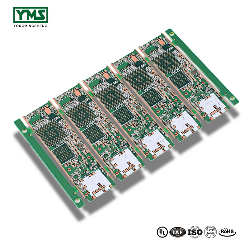
Which has a positive and progressive attitude to customer’s fascination, our enterprise consistently improves our item excellent to satisfy the desires of customers and further focuses on safety, reliability, environmental demands, and innovation of Factory Promotional Green Fr4 Gold Finger Multilayer Pcb Board Fabrication, Welcome your enquiry, most effective service will likely be provided with full heart.
Which has a positive and progressive attitude to customer’s fascination, our enterprise consistently improves our item excellent to satisfy the desires of customers and further focuses on safety, reliability, environmental demands, and innovation of 94v0 Pcb Board, Customized Pcb Circuit Board, Pcb, Aiming to grow to be by far the most experienced supplier within this sector in Uganda, we keep researching on the creating procedure and raising the high quality of our principal merchandise. Till now, the merchandise list has been updated on a regular basis and attracted customers from around the globe. In depth data can be obtained in our web page and you’ll be served with good quality consultant service by our after-sale team. They’re about to make it possible for you to get complete acknowledge about our things and make a satisfied negotiation. Small business check out to our factory in Uganda can also be welcome at any time. Hope to obtain your inquiries to get a happy co-operation.
HDI basic production process:
A、Brown multilayer circuit board to form Browning film on the surface of copper foil layer, and laser drilling on the surface of copper foil to form laser blind hole
B、 drill the multi-layer circuit board to form a mechanical drill hole
C、 The multi-layer circuit board is coated with copper to form a copper layer in the laser blind hole mechanical drilling, and then the multi-layer circuit board is electroplated to thicken the copper layer in the hole
D、The above multilayer circuit board is made of outer graphics, and the surface treatment of etched screen print resistance welding on the outer layer of graphics electroplating is carried out to obtain the finished HDI board
You May Like:
1、How to identify gold on a pcb
Products categories
-
Online Exporter China Shenzhen Supplier One-Sto...
-
High TG FR4 Material PCB BGA Pitch 0.65mm Whole...
-
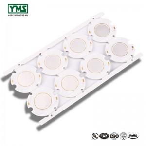
China OEM Customzized 5730 Led Aluminum Pcb,Led...
-
Best-Selling China 6-Layer High Tg Thick Copper...
-

100% Original China Double Side PCB High Tg Man...
-
Wholesale ODM Led Tube Lighting Metal Core Pcb,...


