
Top Suppliers China HDI PCB BGA

We know that we only thrive if we will guarantee our combined cost competiveness and high-quality advantageous at the same time for Top Suppliers China HDI PCB BGA, Welcome to visit us at any time for organization marriage established.
We know that we only thrive if we will guarantee our combined cost competiveness and high-quality advantageous at the same time for China PCB Board, Printed Circuit Board, Our company has already had a lot of top factories and experienced technology teams in China, offering the best products, techniques and services to worldwide customers. Honesty is our principle, qualified operation is our work, service is our goal, and customers’ satisfaction is our future!
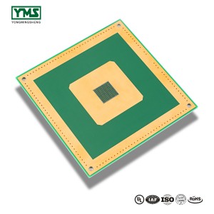
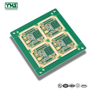
What is HDI PCB
HDI PCB: High density interconnect PCB, are a way of making more room on your printed circuit board to make them more efficient and allow for faster transmission. It’s relatively easy for most enterprising companies that are using printed circuit boards to see how this can benefit them.
Advantages of HDI PCB
The most common reason for using HDI technology is a significant increase in packaging density. The space obtained by finer track structures is available for components. Besides, overall space requirements are reduced will result in smaller board sizes and fewer layers.
Usually FPGA or BGA are available with 1mm or less spacing. HDI technology makes routing and connection easy, especially when routing between pins.
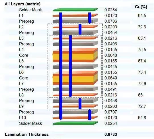
YMS HDI PCB manufacturing capabilities:
| YMS HDI PCB manufacturing capabilities overview | |
| Feature | capabilities |
| Layer Count | 4-60L |
| Available HDI PCB Technology | 1+N+1 |
| 2+N+2 | |
| 3+N+3 | |
| 4+N+4 | |
| 5+N+5 | |
| Any layer | |
| Thickness | 0.3mm-6mm |
| Minimum line Width and Space | 0.05mm/0.05mm(2mil/2mil) |
| BGA PITCH | 0.35mm |
| Min laser Drilled Size | 0.075mm(3nil) |
| Min mechanical Drilled Size | 0.15mm(6mil) |
| Aspect Ratio for laser hole | 0.9:1 |
| Aspect Ratio for through hole | 16:1 |
| Surface Finish | HASL, Lead free HASL,ENIG,Immersion Tin, OSP, Immersion Silver, Gold Finger, Electroplating Hard Gold, Selective OSP,ENEPIG.etc. |
| Via Fill Option | The via is plated and filled with either conductive or non-conductive epoxy then capped and plated over |
| Copper filled, silver filled | |
| Laser via copper plated shut | |
| Registration | ±4mil |
| Solder Mask | Green, Red, Yellow, Blue, White, Black, Purple, Matte Black, Matte green.etc. |

Products categories
-
Reasonable price er For 2layer Fpc Of Led Strips
-
Best-Selling China 6-Layer High Tg Thick Copper...
-
Hot-selling 2019 Hot End Fr4 Smd Flexible Circu...
-
Factory printed circuit board manufacturer adva...
-
Special Design for Shenzhen Multilayer Gold Fin...
-
Quality Inspection for China Good Quality 10 La...


