Big discounting Customized Blank Printed Circuit Board Bare Pcb Boards Electronic Blank Pcb

We take “customer-friendly, quality-oriented, integrative, innovative” as objectives. “Truth and honesty” is our management ideal for Big discounting Customized Blank Printed Circuit Board Bare Pcb Boards Electronic Blank Pcb, We are sincerely wanting forward to creating good cooperative associations with shoppers from in the home and overseas for making a vivid foreseeable future collectively.
We take “customer-friendly, quality-oriented, integrative, innovative” as objectives. “Truth and honesty” is our management ideal for Bare Pcb Boards, Blank Pcb, Printed Circuit Board, Our company has built stable business relationships with many well-known domestic companies as well as oversea customers. With the goal of providing high quality products to customers at low cots, we’ve been committed to improving its capacities in research, development, manufacturing and management. We have honored to receive recognition from our customers. Till now we have now passed ISO9001 in 2005 and ISO/TS16949 in 2008. Enterprises of “quality of survival, the credibility of development” for the purpose, sincerely welcome domestic and foreign businessmen to visit to discuss cooperation.
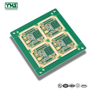
HDI Structures:
1+N+1 – PCBs contain 1 “build-up” of high-density interconnection layers.
i+N+i (i≥2) – PCBs contain 2 or more “build-up” of high density interconnection layers. Microvias on different layers can be staggered or stacked. Copper filled stacked microvia structures are commonly seen in challenging designs.
Any Layer HDI – All the layers of a PCB are high density interconnection layers which allows the conductors on any layer of the PCB to be interconnected freely with copper filled stacked microvia structures (“any layer via”). This provides a reliable interconnect solution for highly complex large pin-count device
You May Like:
2、HDI PCB market supply and demand analysis and circuit advantages
3、How to define the order of HDI board