China Supplier Customized Printed Circuit Board And Pcba Design For

We pursue the administration tenet of “Quality is top-quality, Services is supreme, Popularity is first”, and will sincerely create and share success with all clients for China Supplier Customized Printed Circuit Board And Pcba Design For, Trust us, you might discover a far better solution on car parts industry.
We pursue the administration tenet of “Quality is top-quality, Services is supreme, Popularity is first”, and will sincerely create and share success with all clients for Pcba Board, Pcba Circuit Board, Printing Circuit Board, Our R&D department always designs with new fashion ideas so we could introduce up-to-date fashion styles every month. Our strict production management systems always ensure stable and high quality products. Our trade team provides timely and efficient services. If there are any curiosity and inquiry about our goods, please contact us in time. We would like to establish a business relationship with your honored company.
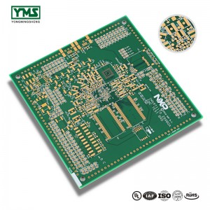
High density interconnect (HDI) PCBs represent one of the fastest-growing segments of the printed circuit board market. Because of its higher circuitry density, the HDI PCB design can incorporate finer lines and spaces, smaller vias and capture pads, and higher connection pad densities. A high-density PCB features blind and buried vias and often contains microvias that are .006 in diameter or even less.
1.Multi-step HDI enables the connection between any layers;
2.Cross-layer laser processing can enhance the quality level of multi-step HDI;
3.The combination of HDI and high-frequency materials, metal-based laminates, FPC and other special laminates and processes enable the needs of high density and high frequency, high heat conducting, or 3D assembly.
You May Like:
1、The application range and circuit advantage of HDI board are introduced
2、PCB production skills: HDI board CAM production method
3、PCB design of 1 step, 2 step and 3step HDI