Chinese Professional China Gold Supplier Fiber Cement Board
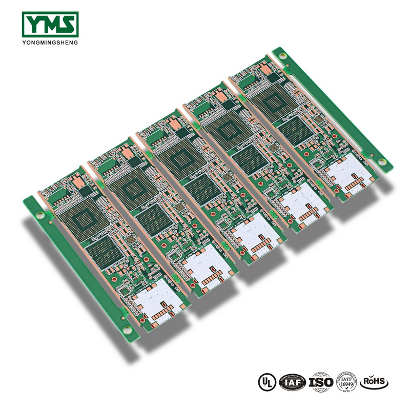
Our eternal pursuits are the attitude of “regard the market, regard the custom, regard the science” as well as theory of “quality the basic, have faith in the initial and administration the advanced” for Chinese Professional China Gold Supplier Fiber Cement Board, We welcome new and outdated clients to get in touch with us by cell phone or send us inquiries by mail for long term business relationships and accomplishing mutual results.
Our eternal pursuits are the attitude of “regard the market, regard the custom, regard the science” as well as theory of “quality the basic, have faith in the initial and administration the advanced” for Cement Board, China Fiber Cement Board, We honor ourselves as a company that comprises of a strong team of professionals who are innovative and well experienced in the international trading, business development and product advancement. Moreover, the company stays unique among its competitors due to its superior standard of quality in production, and its efficiency and flexibility in business support.
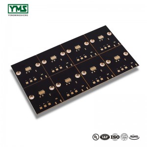
Goldfinger design in PCB
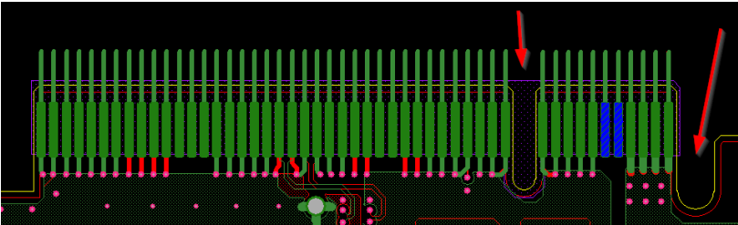
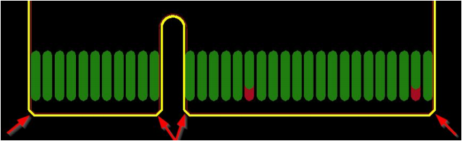
Goldfinger is an electrical interface. The common packaging form and appearance of PCB are as follows. When the appearance and packaging similar to the figure below are seen in the PCB design, the first reaction is to see them on the boardGold finger.
The easier way for goldfinger to judge is to have both the TOP and BOTTOM of the device
PIN device;It will look like the u-slot in the picture below.
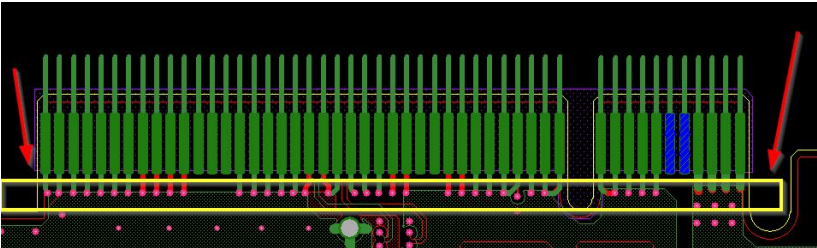
When there is a goldfinger on the board, you need to work on the details of the goldfinger.
Details of goldfinger in PCB:
1) in order to increase the wear resistance of goldfinger, goldfinger usually needs to be plated with hard gold.
2) goldfinger needs chamfering, usually 45°, other angles such as 20°, 30°, etc.
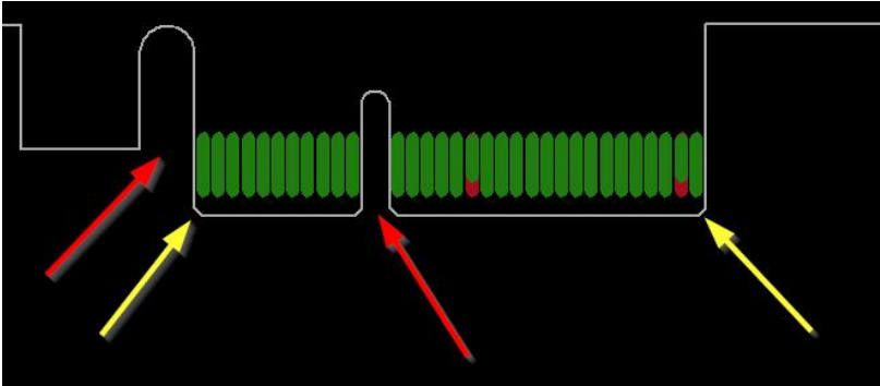
If there is no chamfer in the design, there is a problem.In the figure below, the arrow is 45 degrees
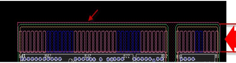
chamfering
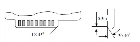
The 45° chamfering Angle in PCB is shown in the following figure:
3) goldfinger needs to do the whole block of anti-welding window opening treatment, and the PIN does not need to open the steel net;
4) a minimum distance of 14mil from the tip of finger is required for the sink tin and silver welding pads;Recommended design
When the pad is more than 1mm away from the finger position, including the through hole pad;
5) do not coat goldfinger with copper;
Below is a goldfinger design for reference
6) all layers of the inner layer of goldfinger need to be copper whittled, usually with a width of 3mm;
It can be done with half finger and whole finger.In pci-e design, there are also fingers
Remove all copper from the mingoldfinger area;
Goldfinger’s resistance will be low, and cupping (hollowing out under the finger) will reduce it
The impedance difference between the impedance line and the impedance line is also beneficial to ESD.
Suggestion: cut all the copper under the goldfinger welding pad
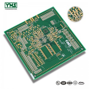
HDI basic production process:
A、Brown multilayer circuit board to form Browning film on the surface of copper foil layer, and laser drilling on the surface of copper foil to form laser blind hole
B、 drill the multi-layer circuit board to form a mechanical drill hole
C、 The multi-layer circuit board is coated with copper to form a copper layer in the laser blind hole mechanical drilling, and then the multi-layer circuit board is electroplated to thicken the copper layer in the hole
D、The above multilayer circuit board is made of outer graphics, and the surface treatment of etched screen print resistance welding on the outer layer of graphics electroplating is carried out to obtain the finished HDI board
You May Like:
1、How to identify gold on a pcb
4、The main causes of PCB board deformation and rupture