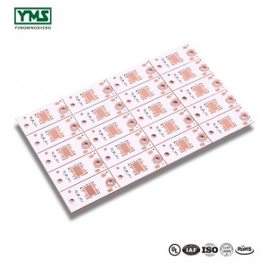
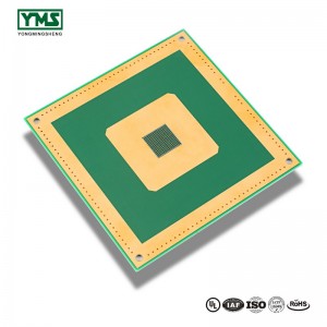
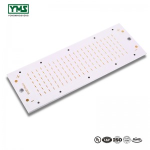
Factory source 94v0 Dual Layer Aluminium Metal Core Pcb,Fr4 Clad Copper Clad Pcb Assembly

We’ve one of the most advanced generation tools, experienced and qualified engineers and workers, recognized good quality manage systems and a friendly skilled product sales workforce pre/after-sales support for Factory source 94v0 Dual Layer Aluminium Metal Core Pcb,Fr4 Clad Copper Clad Pcb Assembly, should you have any query or wish to place an initial buy be sure to don’t wait to call us.
We’ve one of the most advanced generation tools, experienced and qualified engineers and workers, recognized good quality manage systems and a friendly skilled product sales workforce pre/after-sales support for Aluminium Metal Core Pcb, Copper Clad Pcb, Fr4 Clad Copper Clad Pcb, We hope to have long-term cooperation relationships with our clients. If you are interested in any of our items, be sure to do not hesitate to send enquiry to us/company name. We ensure that you can be totally satisfied with our best solutions!
Copper base Board production process
- Provide the copper plate have pretreated
- UV ink is printed on the bending part of copper plate
- The surface of copper plate is browned by using browning liquid
- Press and drill copper plate covered with UV ink
- Electroplate the first finished product
- Make outer layer on copper plate
- Solder mask printing on copper substrate
- V – CUT the second finished product
- The bending position of copper plate is surface treated and the finished product is obtained
- Check up case ,packing and shipping
You May Like:
1、PCB hole copper fracture reason
2、What are the requirements for copper thickness of PCB orifice
3、9 attention points of copper application