Low MOQ for Black Printed Circuit Boards - Manufacturer for printed circuit board and pcb design from shenzhen pcb – Yongmingsheng
Low MOQ for Black Printed Circuit Boards - Manufacturer for printed circuit board and pcb design from shenzhen pcb – Yongmingsheng Detail:
The shopper satisfaction is our primary focus on. We uphold a consistent level of professionalism, quality, credibility and repair for Manufacturer for printed circuit board and pcb design from shenzhen pcb, To deliver prospects with excellent equipment and providers, and frequently create new machine is our company’s organization objectives. We look forward for your cooperation.
The shopper satisfaction is our primary focus on. We uphold a consistent level of professionalism, quality, credibility and repair for , Our company regards “reasonable prices, efficient production time and good after-sales service” as our tenet. We hope to cooperate with more customers for mutual development and benefits. We welcome potential buyers to contact us.
Goldfinger design in PCB
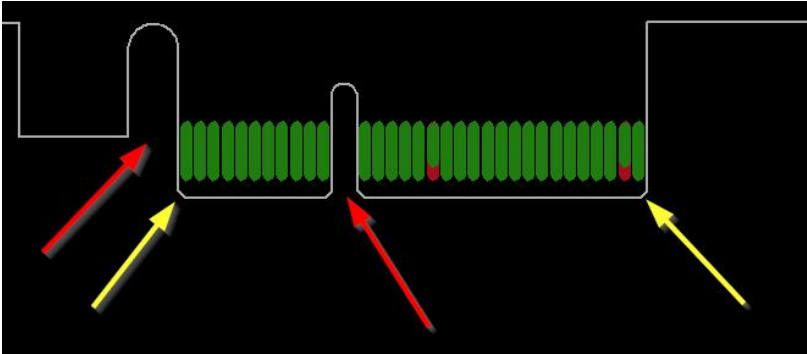
Goldfinger is an electrical interface. The common packaging form and appearance of PCB are as follows. When the appearance and packaging similar to the figure below are seen in the PCB design, the first reaction is to see them on the boardGold finger.
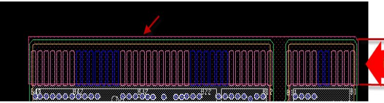
The easier way for goldfinger to judge is to have both the TOP and BOTTOM of the device
PIN device;It will look like the u-slot in the picture below.
When there is a goldfinger on the board, you need to work on the details of the goldfinger.
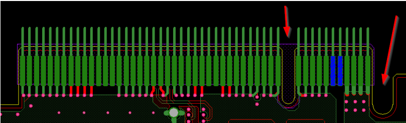
Details of goldfinger in PCB:
1) in order to increase the wear resistance of goldfinger, goldfinger usually needs to be plated with hard gold.
2) goldfinger needs chamfering, usually 45°, other angles such as 20°, 30°, etc.
If there is no chamfer in the design, there is a problem.In the figure below, the arrow is 45 degrees
chamfering
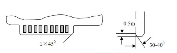
The 45° chamfering Angle in PCB is shown in the following figure:
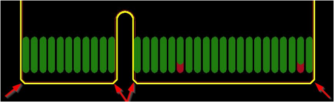
3) goldfinger needs to do the whole block of anti-welding window opening treatment, and the PIN does not need to open the steel net;
4) a minimum distance of 14mil from the tip of finger is required for the sink tin and silver welding pads;Recommended design
When the pad is more than 1mm away from the finger position, including the through hole pad;
5) do not coat goldfinger with copper;
Below is a goldfinger design for reference
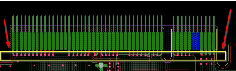
6) all layers of the inner layer of goldfinger need to be copper whittled, usually with a width of 3mm;
It can be done with half finger and whole finger.In pci-e design, there are also fingers
Remove all copper from the mingoldfinger area;
Goldfinger’s resistance will be low, and cupping (hollowing out under the finger) will reduce it
The impedance difference between the impedance line and the impedance line is also beneficial to ESD.
Suggestion: cut all the copper under the goldfinger welding pad
HDI basic production process:
A、Brown multilayer circuit board to form Browning film on the surface of copper foil layer, and laser drilling on the surface of copper foil to form laser blind hole
B、 drill the multi-layer circuit board to form a mechanical drill hole
C、 The multi-layer circuit board is coated with copper to form a copper layer in the laser blind hole mechanical drilling, and then the multi-layer circuit board is electroplated to thicken the copper layer in the hole
D、The above multilayer circuit board is made of outer graphics, and the surface treatment of etched screen print resistance welding on the outer layer of graphics electroplating is carried out to obtain the finished HDI board
You May Like:
1、How to identify gold on a pcb
4、The main causes of PCB board deformation and rupture
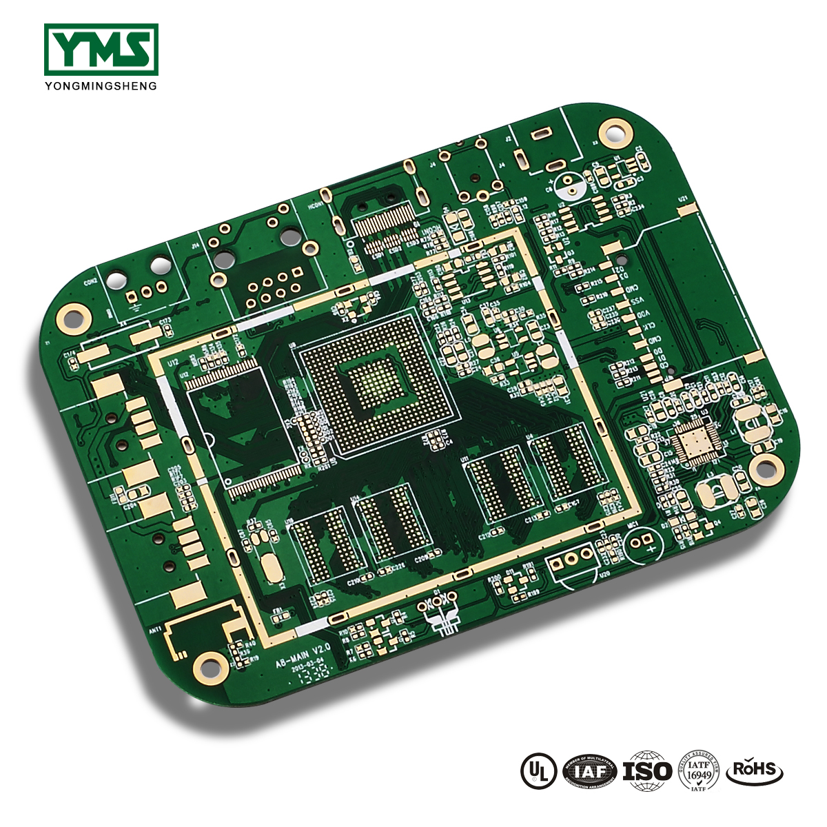
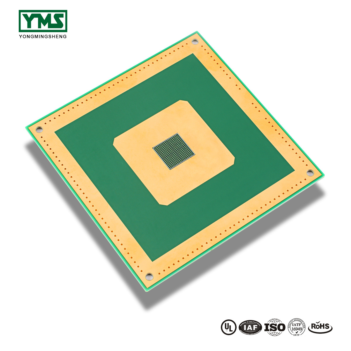
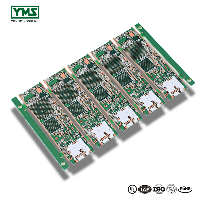
Product detail pictures:
Related Product Guide:
A ‘painless’ approach to energy: Upper Nappan home provides proof that living off-grid can be comfortable | Regional | News | Hdi Pcb
‘The US government has checked out on renewables’: can cities fill the gap? | Cities | 1.2m 2layer Led Pcb
To create much more price for clients is our company philosophy; purchaser growing is our working chase for Low MOQ for Black Printed Circuit Boards - Manufacturer for printed circuit board and pcb design from shenzhen pcb – Yongmingsheng , The product will supply to all over the world, such as: America, Paraguay, Romania, We welcome customers from all over the world come to discuss business. We supply high quality solutions, reasonable prices and good services. We hope to sincerely build business relationships with customers from at home and abroad, jointly striving for a resplendent tomorrow.
On this website, product categories is clear and rich, I can find the product I want very quickly and easily, this is really very good!