
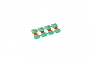
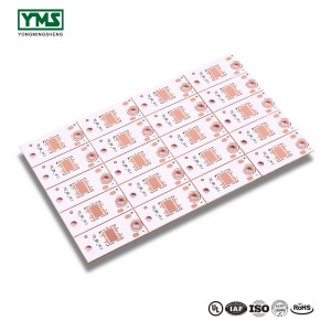
ODM Manufacturer Muti Layers Pcb Card Mainboard

With this motto in mind, we’ve come to be one of quite possibly the most technologically innovative, cost-efficient, and price-competitive manufacturers for ODM Manufacturer Muti Layers Pcb Card Mainboard, We welcome new and previous consumers from all walks of lifestyle to speak to us for upcoming business enterprise associations and mutual results!
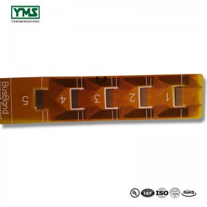
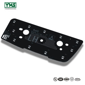
With this motto in mind, we’ve come to be one of quite possibly the most technologically innovative, cost-efficient, and price-competitive manufacturers for Card Pcb, Mainboard Pcb, Mutilayers Pcb, Company name, is always regarding quality as company’ s foundation, seeking for development via high degree of credibility , abiding by ISO quality management standard strictly, creating top-ranking company by spirit of progress-marking honesty and optimism.
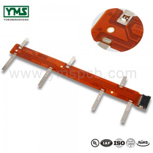
The connecting finger is the connecting element on the memory stick and the memory slot through which all the signals are transmitted.The golden finger is composed of many golden conductive contact plates, which are gold plated on the surface and arranged like fingers, so it is called “golden finger”.Gold fingers are actually coated with gold by a special process on a copper clad plate, because of its strong oxidation resistance and conductivity.
Searches related to PCB gold finger
3、10 Layer High Tg Immersion gold Boad
Products categories
-
China wholesale printed circuit board manufactu...
-
Cheap PriceList for Pcb Double-side Powerbank Pcb
-
Reasonable price Pcb Through Hole Machine,Metal...
-
China Gold Supplier for China Decorative Basebo...
-
Good Quality Led Borad Led Light Board Led Bulb...
-
OEM/ODM China 30oz Enig Extreme Copper Pcb,Heav...


