
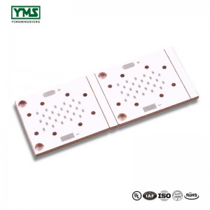
Popular Design for China Smart Electronics Mobile Phone PCB Board Android PCBA PCB Circuit Boards PCB

In order to best meet client’s needs, all of our operations are strictly performed in line with our motto “High Quality, Competitive Price, Fast Service” for Popular Design for China Smart Electronics Mobile Phone PCB Board Android PCBA PCB Circuit Boards PCB, With our rules of ” small business status, partner trust and mutual benefit”, welcome all of you to definitely get the job done jointly , mature jointly.
In order to best meet client’s needs, all of our operations are strictly performed in line with our motto “High Quality, Competitive Price, Fast Service” for China PCB Board, Pcb Circuit Boards, Our production have been exported to more than 30 countries and regions as first hand source with lowest price. We sincerely welcome customers from both at home and abroad to come to negotiate business with us.
Printed Circuit Board Introduction
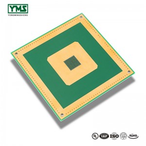
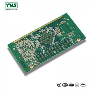
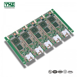
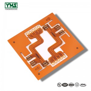
A printed circuit board (PCB) mechanically supports and electrically connects electrical or electronic components using conductive tracks, pads and other features etched from one or more sheet layers of copper laminated onto and/or between sheet layers of a non-conductive substrate. Components are generally soldered onto the PCB to both electrically connect and mechanically fasten them to it.PCBs can be single-sided (one copper layer), double-sided (two copper layers on both sides of one substrate layer), or multi-layer (outer and inner layers of copper, alternating with layers of substrate). Multi-layer PCBs allow for much higher component density, because circuit traces on the inner layers would otherwise take up surface space between components. The rise in popularity of multilayer PCBs with more than two, and especially with more than four, copper planes was concurrent with the adoption of surface mount technology.

What is the difference between a Countersink and a Counterbore?

YMS Normal PCB manufacturing capabilities:
| YMS Normal PCB manufacturing capabilities overview | ||
| Feature | capabilities | |
| Layer Count | 1-60L | |
| Available Normal PCB Technology | Through hole with Aspect Ratio 16:1 | |
| buried and blind via | ||
| Hybrid | High Frequency Material such as RO4350B and FR4 Mix etc. | |
| High Speed Material such as M7NE and FR4 Mix etc. | ||
| Material | CEM- | CEM-1;CEM-2;CEM-4;CEM-5.etc |
| FR4 | EM827, 370HR, S1000-2, IT180A, IT158, S1000 / S1155, R1566W, EM285, TU862HF,NP170G etc. | |
| High Speed | Megtron6, Megtron4, Megtron7,TU872SLK, FR408HR,N4000-13 Series,MW4000,MW2000,TU933 etc. | |
| High Frequency | Ro3003, Ro3006, Ro4350B, Ro4360G2, Ro4835, CLTE, Genclad, RF35, FastRise27 etc. | |
| Others | Polyimide, Tk, LCP, BT, C-ply, Fradflex, Omega , ZBC2000,PEEK,PTFE,ceramic-based etc. | |
| Thickness | 0.3mm-8mm | |
| Max.copper Thickness | 10OZ | |
| Minimum line Width and Space | 0.05mm/0.05mm(2mil/2mil) | |
| BGA PITCH | 0.35mm | |
| Min mechanical Drilled Size | 0.15mm(6mil) | |
| Aspect Ratio for through hole | 16:1 | |
| Surface Finish | HASL, Lead free HASL,ENIG,Immersion Tin, OSP, Immersion Silver, Gold Finger, Electroplating Hard Gold, Selective OSP,ENEPIG.etc. | |
| Via Fill Option | The via is plated and filled with either conductive or non-conductive epoxy then capped and plated over(VIPPO) | |
| Copper filled, silver filled | ||
| Registration | ±4mil | |
| Solder Mask | Green, Red, Yellow, Blue, White, Black, Purple, Matte Black, Matte green.etc. | |
You May Like:
1、Summary of matters needing attention in circuit board welding

Products categories
-
Trending Products Heavy Copper Pcb Circuit Boar...
-
Cheap price Multilayer Fr-4 Blind Buried Hole I...
-
Manufacturer for printed circuit board and pcb ...
-
Best quality Pcb Customized Aluminum Pcb Rigid ...
-
OEM Manufacturer Shenzhen Precision Circuit Boa...
-
OEM Manufacturer Shenzhen Oem Fpc Customized Fp...


