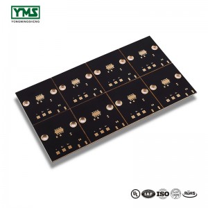
China Factory for China HDI PCB Multilayer Printed Circuit Board Blind and Buried Holes Immersion Gold

We are ready to share our knowledge of marketing worldwide and recommend you suitable products at most aggressive costs. So Profi Tools offer you finest benefit of money and we are ready to produce alongside one another with China Factory for China HDI PCB Multilayer Printed Circuit Board Blind and Buried Holes Immersion Gold, We sincerely welcome overseas customers to consult for the long-term cooperation and the mutual development.
We are ready to share our knowledge of marketing worldwide and recommend you suitable products at most aggressive costs. So Profi Tools offer you finest benefit of money and we are ready to produce alongside one another with China PCB, Printed Circuit Board, Our company has a skillful sales team, strong economic foundation, great technical force, advanced equipment, complete testing means, and excellent after-sales services. Our products have beautiful appearance, fine workmanship and superior quality and win the unanimous approvals of the customers all over the world.
What is HDI PCBs?
High density interconnect (HDI) PCBs represent one of the fastest-growing segments of the printed circuit board market. Because of its higher circuitry density, the HDI PCB design can incorporate finer lines and spaces, smaller vias and capture pads, and higher connection pad densities. A high-density PCB features blind and buried vias and often contains microvias that are .006 in diameter or even less.
1.Multi-step HDI enables the connection between any layers;
2.Cross-layer laser processing can enhance the quality level of multi-step HDI;
3.The combination of HDI and high-frequency materials, metal-based laminates, FPC and other special laminates and processes enable the needs of high density and high frequency, high heat conducting, or 3D assembly.

YMS HDI PCB manufacturing capabilities:
| YMS HDI PCB manufacturing capabilities overview | |
| Feature | capabilities |
| Layer Count | 4-60L |
| Available HDI PCB Technology | 1+N+1 |
| 2+N+2 | |
| 3+N+3 | |
| 4+N+4 | |
| 5+N+5 | |
| Any layer | |
| Thickness | 0.3mm-6mm |
| Minimum line Width and Space | 0.05mm/0.05mm(2mil/2mil) |
| BGA PITCH | 0.35mm |
| Min laser Drilled Size | 0.075mm(3nil) |
| Min mechanical Drilled Size | 0.15mm(6mil) |
| Aspect Ratio for laser hole | 0.9:1 |
| Aspect Ratio for through hole | 16:1 |
| Surface Finish | HASL, Lead free HASL,ENIG,Immersion Tin, OSP, Immersion Silver, Gold Finger, Electroplating Hard Gold, Selective OSP,ENEPIG.etc. |
| Via Fill Option | The via is plated and filled with either conductive or non-conductive epoxy then capped and plated over |
| Copper filled, silver filled | |
| Laser via copper plated shut | |
| Registration | ±4mil |
| Solder Mask | Green, Red, Yellow, Blue, White, Black, Purple, Matte Black, Matte green.etc. |
You May Like:
1、The application range and circuit advantage of HDI board are introduced
What does HDI stand for in electronics?
HDI stands for High Density Interconnector. A circuit board which has a higher wiring density per unit area as opposed to conventional board is called as HDI PCB. HDI PCBs have finer spaces and lines, minor vias and capture pads and higher connection pad density.
What is staggered Via?
Staggered Vias are the most common and economical form of microvias. However, staggered microvias require more space as a result of not being built around the same core. Via Fill, or copper filled via , increases the thermal conductivity of the via by closing via hole with epoxy using a specific fabrication process.
Search for: What is staggered Via?
What is a stacked via?
The Stacked Via:
A stacked via consists of multiple vias layered directly on top of each other. Each via is first drilled and then metalized, leaving a small annular ring at the top and bottom to ensure electrical connection. This annular ring is typically very narrow – as thin as .