
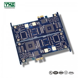
China Manufacturer for China Professional HDI Supplier High Tg PCB Circuit Board Multilayer Buried and Blind Via Holes PCB with RoHS

We believe in: Innovation is our soul and spirit. High-quality is our life. Purchaser need is our God for China Manufacturer for China Professional HDI Supplier High Tg PCB Circuit Board Multilayer Buried and Blind Via Holes PCB with RoHS, Our aim is to help customers realize their goals. We are making great efforts to achieve this win-win situation and sincerely welcome you to join us.
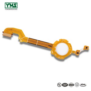
We believe in: Innovation is our soul and spirit. High-quality is our life. Purchaser need is our God for China Printed Circuit Board, Fpc, We integrate design, manufacture and export together with more than 100 skillful workers, strict quality controlling system and experienced technology.We keep long term business relationships with wholesaler and distributors form more than 50 countries, such as USA, UK, Canada, Europe and Africa etc.
What is HDI PCBs?
High density interconnect (HDI) PCBs represent one of the fastest-growing segments of the printed circuit board market. Because of its higher circuitry density, the HDI PCB design can incorporate finer lines and spaces, smaller vias and capture pads, and higher connection pad densities. A high-density PCB features blind and buried vias and often contains microvias that are .006 in diameter or even less.
1.Multi-step HDI enables the connection between any layers;
2.Cross-layer laser processing can enhance the quality level of multi-step HDI;
3.The combination of HDI and high-frequency materials, metal-based laminates, FPC and other special laminates and processes enable the needs of high density and high frequency, high heat conducting, or 3D assembly.

YMS HDI PCB manufacturing capabilities:
| YMS HDI PCB manufacturing capabilities overview | |
| Feature | capabilities |
| Layer Count | 4-60L |
| Available HDI PCB Technology | 1+N+1 |
| 2+N+2 | |
| 3+N+3 | |
| 4+N+4 | |
| 5+N+5 | |
| Any layer | |
| Thickness | 0.3mm-6mm |
| Minimum line Width and Space | 0.05mm/0.05mm(2mil/2mil) |
| BGA PITCH | 0.35mm |
| Min laser Drilled Size | 0.075mm(3nil) |
| Min mechanical Drilled Size | 0.15mm(6mil) |
| Aspect Ratio for laser hole | 0.9:1 |
| Aspect Ratio for through hole | 16:1 |
| Surface Finish | HASL, Lead free HASL,ENIG,Immersion Tin, OSP, Immersion Silver, Gold Finger, Electroplating Hard Gold, Selective OSP,ENEPIG.etc. |
| Via Fill Option | The via is plated and filled with either conductive or non-conductive epoxy then capped and plated over |
| Copper filled, silver filled | |
| Laser via copper plated shut | |
| Registration | ±4mil |
| Solder Mask | Green, Red, Yellow, Blue, White, Black, Purple, Matte Black, Matte green.etc. |
You May Like:
1、The application range and circuit advantage of HDI board are introduced
2、PCB production skills: HDI board CAM production method
3、PCB design of 1 step, 2 step and 3step HDI

Products categories
-
2019 wholesale price One-stop Pcb Assembly For ...
-
Top Quality New rigid led strip /led rigid stri...
-
Online Exporter SGS approved customized 94v0 FP...
-
Board-300x300.jpg)
Factory wholesale Doorbell Pcb Heavy Copper Pcb...
-
Factory made hot-sale 2layer Fpc Flexible Print...
-
Factory supplied Non Slip Flexible Chopping Boa...


Board-300x300.jpg)

