
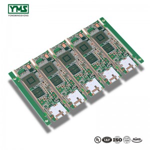
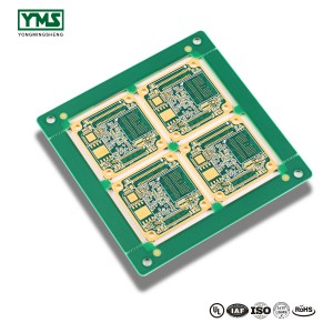
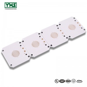
Best Price for 4 Layers Hdi Rigid-flex Pcb With 4-layer Rigid Flex Pcb
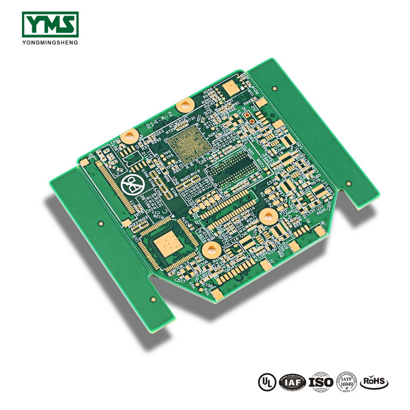
Our products and solutions are extensively identified and trustworthy by users and can meet up with continuously developing financial and social requirements for Best Price for 4 Layers Hdi Rigid-flex Pcb With 4-layer Rigid Flex Pcb, Customer pleasure is our main objective. We welcome you to set up business relation with us. For even further information, make sure you will not wait to contact with us.
Our products and solutions are extensively identified and trustworthy by users and can meet up with continuously developing financial and social requirements for 4 Layers Hdi Rigid-flex Pcb, 4-layer Rigid Flex Pcb, Rigid-Flex Pcb, now we have all day online sales to make sure the pre-sale and after-sale service in time. With all these supports, we can serve every customer with quality product and timely shipping with highly responsibility. Being a young growing company, we might not the best, but we are trying our best to be your good partner.
HDI Board production process:
At present, HDI board interconnection between layer and layer is mainly the following design: Staggered holes interconnection, Cross-layer interconnection, ladder interconnection and superposition holes interconnection. Among them, the superposition holes interconnection occupy the least space. There is a research suggests that reducing the number of through holes and increasing the number of blind holes can effectively improve the wiring density. And in the superposition interconnection, the methods of electroplating and resin plug are mainly used, especially the electroplating hole filling method which has more obvious advantages like high reliability and good conduction performance.
Therefore, superposition interconnection is the most widely used design method for blind holes design. The process of stacking between layers is as follows: first blind hole is made, then second blind hole is made after lamination, then multi-blind hole is made according to this method, and the interconnection between layers is realized by electroplating hole filling method.
On the whole, the production process of HDI plate is complex, which needs to be completed after many times of production for a long time. It’s not only high requirements for the accuracy and shrinkage control of each layer, but also high standards in materials, equipment, environment and technical personnel.
You May Like:
2、Drill holes for printed circuit boards
3、Multi-layer circuit board composition
Products categories
-
2019 wholesale price Copper Base Metal Core Pcb...
-
Factory supplied Iso 9001 Certificate Manufactu...
-
Factory Promotional Green Fr4 Gold Finger Multi...
-
Manufacturer for printed circuit board and pcb ...
-
Competitive Price for electronic boards,pcb rev...
-
Trending Products Performance Low Cost 1 2 Laye...


