
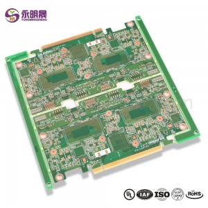
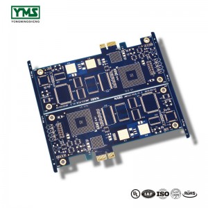
China Cheap price Customized Made Aluminum Bare Board For Led Manufacturing
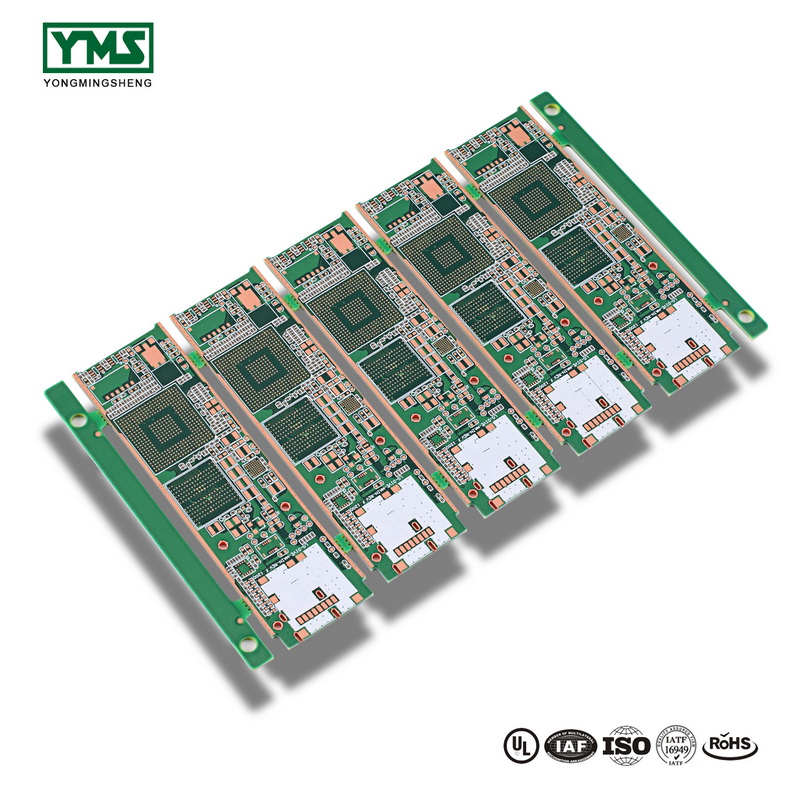
We have now a hugely efficient team to deal with inquiries from buyers. Our goal is “100% client gratification by our solution high-quality, rate & our team service” and take pleasure in a great popularity among clients. With several factories, we will provide a wide assortment of China Cheap price Customized Made Aluminum Bare Board For Led Manufacturing, We now have substantial goods source and also the rate is our advantage. Welcome to inquire about our merchandise.
We have now a hugely efficient team to deal with inquiries from buyers. Our goal is “100% client gratification by our solution high-quality, rate & our team service” and take pleasure in a great popularity among clients. With several factories, we will provide a wide assortment of Aluminum Pcb Bare Board, Customized Made, Led Lighting, Our R&D department always designs with new fashion ideas so we could introduce up-to-date fashion styles every month. Our strict production management systems always ensure stable and high quality goods. Our trade team provides timely and efficient services. If there are any curiosity and inquiry about our products, remember to contact us in time. We would like to establish a business relationship with your honored company.
HDI basic production process:
A、Brown multilayer circuit board to form Browning film on the surface of copper foil layer, and laser drilling on the surface of copper foil to form laser blind hole
B、 drill the multi-layer circuit board to form a mechanical drill hole
C、 The multi-layer circuit board is coated with copper to form a copper layer in the laser blind hole mechanical drilling, and then the multi-layer circuit board is electroplated to thicken the copper layer in the hole
D、The above multilayer circuit board is made of outer graphics, and the surface treatment of etched screen print resistance welding on the outer layer of graphics electroplating is carried out to obtain the finished HDI board
You May Like:
1、How to identify gold on a pcb
Products categories
-
China Supplier China Single-Sided CREE LED PCB ...
-
PriceList for China OEM ODM FPC Flexible Cable ...
-
Reasonable price Pcb Through Hole Machine,Metal...
-
Trending Products Performance Low Cost 1 2 Laye...
-
China Wholesale China LED Main Board House Appl...
-
ODM Manufacturer Muti Layers Pcb Card Mainboard


