
Factory source Blind And Buried Hole Pcb - 8Layer 2 Step HDI Board | YMSPCB – Yongmingsheng
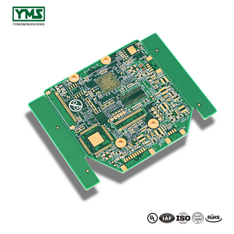
Factory source Blind And Buried Hole Pcb - 8Layer 2 Step HDI Board | YMSPCB – Yongmingsheng Detail:
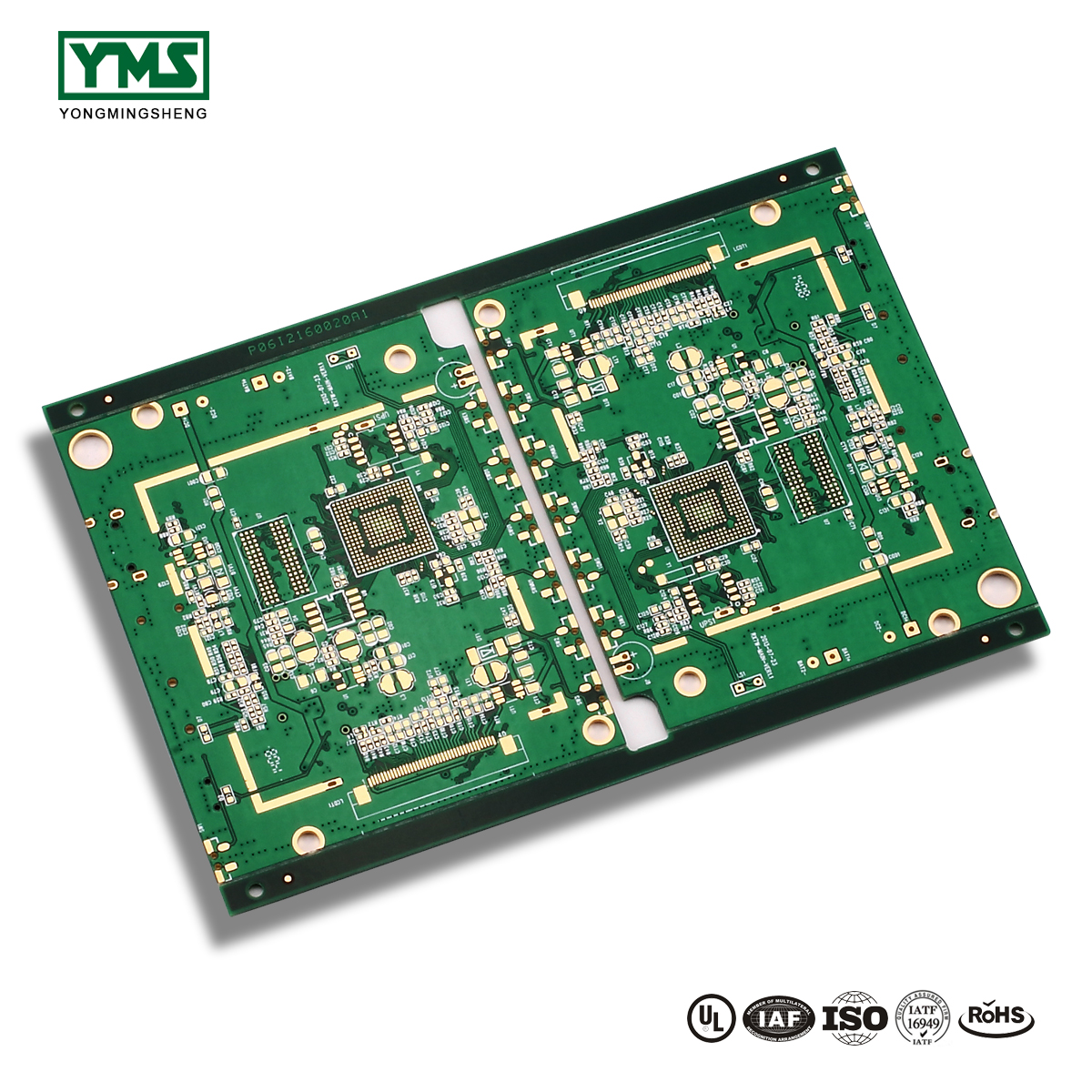
HDI Board production process:
At present, HDI board interconnection between layer and layer is mainly the following design: Staggered holes interconnection, Cross-layer interconnection, ladder interconnection and superposition holes interconnection. Among them, the superposition holes interconnection occupy the least space. There is a research suggests that reducing the number of through holes and increasing the number of blind holes can effectively improve the wiring density. And in the superposition interconnection, the methods of electroplating and resin plug are mainly used, especially the electroplating hole filling method which has more obvious advantages like high reliability and good conduction performance.
Therefore, superposition interconnection is the most widely used design method for blind holes design. The process of stacking between layers is as follows: first blind hole is made, then second blind hole is made after lamination, then multi-blind hole is made according to this method, and the interconnection between layers is realized by electroplating hole filling method.
On the whole, the production process of HDI plate is complex, which needs to be completed after many times of production for a long time. It’s not only high requirements for the accuracy and shrinkage control of each layer, but also high standards in materials, equipment, environment and technical personnel.
You May Like:
2、Drill holes for printed circuit boards
3、Multi-layer circuit board composition
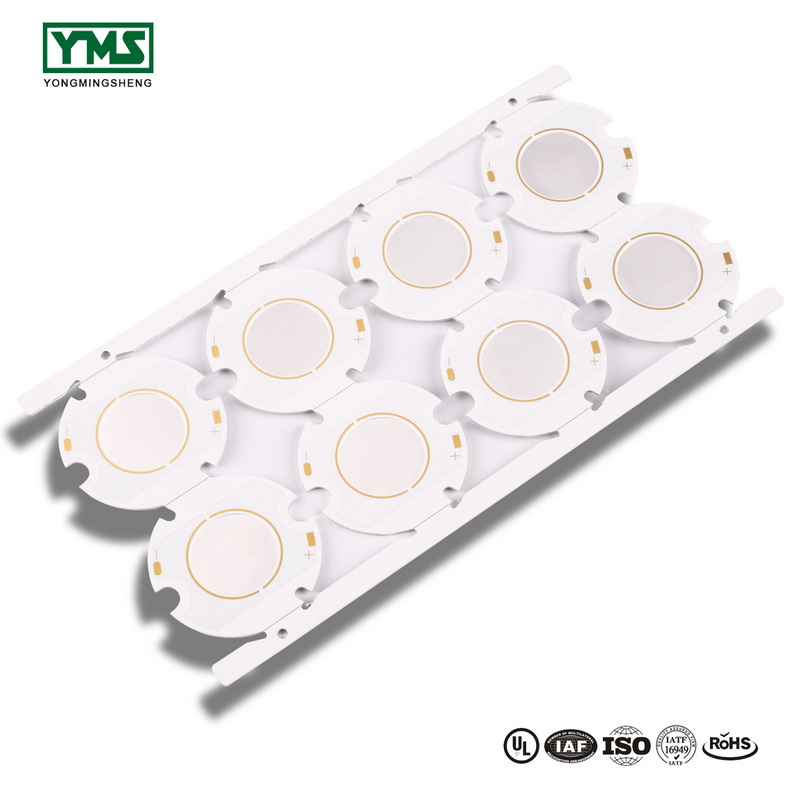
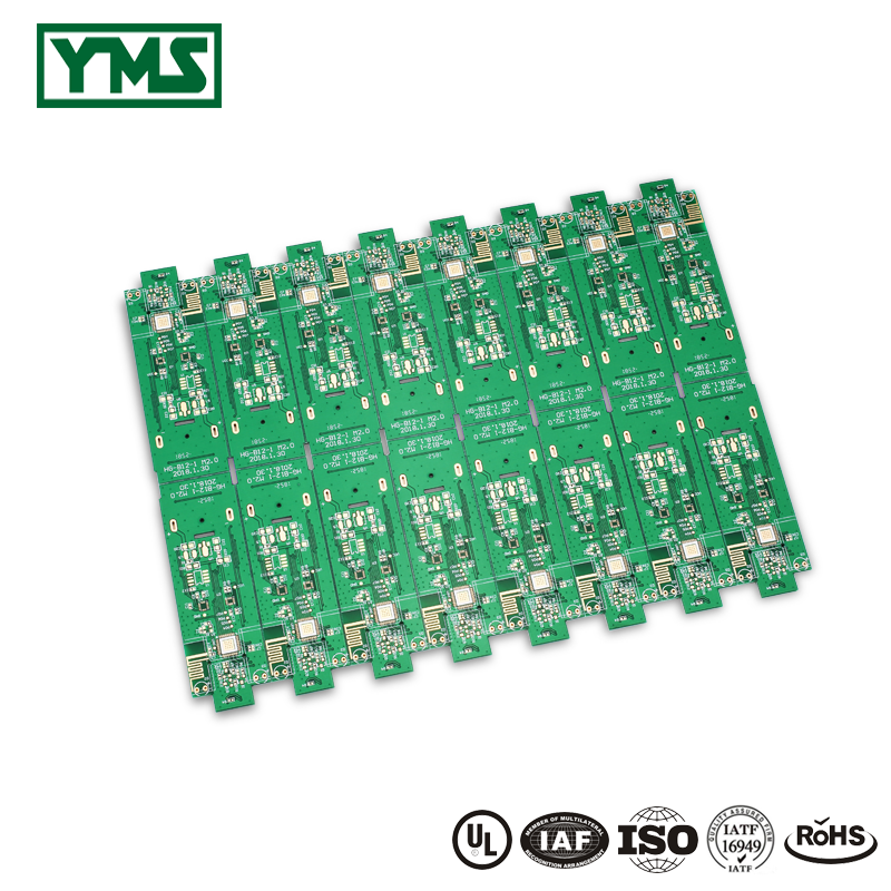
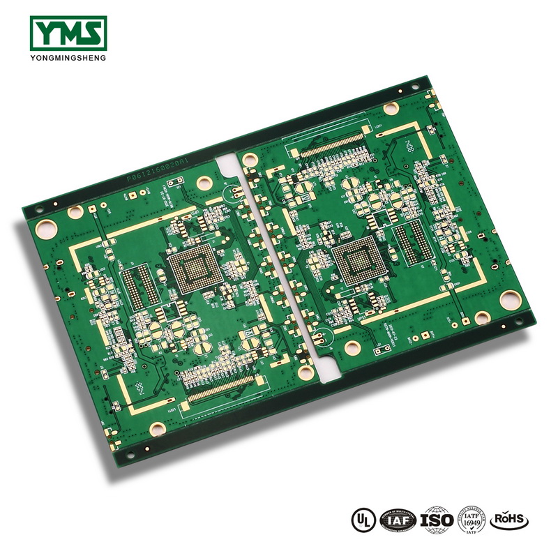
Product detail pictures:
Related Product Guide:
High Density Interconnect (HID) PCB Market: Key Players and Production Information analysis | Hdi Pcb
Calls for frozen pipes strain plumbers | Local News | Copper Base Board
Our business puts emphasis over the administration, the introduction of talented staff, plus the construction of employees building, striving hard to boost the standard and liability consciousness of staff members. Our corporation successfully attained IS9001 Certification and European CE Certification of Factory source Blind And Buried Hole Pcb - 8Layer 2 Step HDI Board | YMSPCB – Yongmingsheng , The product will supply to all over the world, such as: Holland, Wellington, Roman, Good quality and reasonable price have brought us stable customers and high reputation. Providing 'Quality Products, Excellent Service, Competitive Prices and Prompt Delivery', we are now looking forward to even greater cooperation with overseas customers based on mutual benefits. We'll work whole-heartedly to improve our solutions and services. We also promise to work jointly with business partners to elevate our cooperation to a higher level and share success together. Warmly welcome you to visit our factory sincerely.
The factory workers have rich industry knowledge and operational experience, we learned a lot in working with them,we are extremely grateful that we can encount a good company has excellent wokers.
Products categories
-
Good Wholesale VendorsThick Gold Pcb - The Mir...
-
Personlized ProductsBlank Printed Circuit Board...
-
Factory Outlets Hi-Pot Withstand Copper Base Pc...
-
Factory Price High Thermal Conductivity - 6 La...
-
2017 China New Design Flex+Rigid - Quots for C...
-
Special Design for Thermoelectric Copper Base P...


