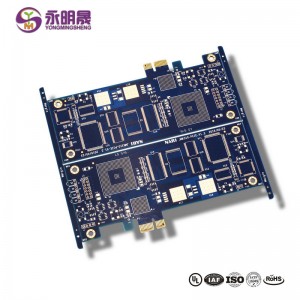
Hot Sale for China 94V0 PCB Board, Fr4 94V0 PCB Circuit Boards, UPS PCB Manufacturer, Normal double side, PCB Solutions, PCB Board Making.
Board28.jpg)
Persisting in “High high quality, Prompt Delivery, Aggressive Price”, we’ve established long-term cooperation with clients from the two overseas and domestically and get new and old clients’ superior comments for Hot Sale for China 94V0 PCB Board, Fr4 94V0 PCB Circuit Boards, UPS PCB Manufacturer, LED PCB Board, Multilayer PCB, PCB Solutions, PCB Board Making., Our enterprise insists on innovation to promote the sustainable development of company, and make us become the domestic high-quality suppliers.
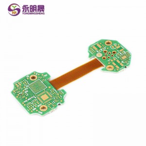
Persisting in “High high quality, Prompt Delivery, Aggressive Price”, we’ve established long-term cooperation with clients from the two overseas and domestically and get new and old clients’ superior comments for China PCB Fabrication, Printed Circuit Board, Satisfaction and good credit to every customer is our priority. We focus on every detail of order processing for customers till they have received safe and sound merchandise with good logistics service and economical cost. Depending on this, our goods are sold very well in the countries in Africa, the Mid-East and Southeast Asia.
Heavy Copper PCB are printed circuit boards with 3 or more ounces of finished copper in the inner and/or outer layers.
While there is no standard definition of Heavy Copper, it is generally accepted that if 3 ounces (oz) of copper or more is used on the internal and external layers of a printed circuit board, it is called a heavy copper PCB. Any circuit with a copper thickness of more than 4 oz per square foot (ft2) is also categorized as a heavy copper PCB.
The construction of a heavy copper circuit endows a board with benefits such as:
- Increased endurance to thermal strains.
- Increased current carrying capacity.
- Increased mechanical strength at connector sites and in PTH holes.
- Use of exotic materials to their full potential without circuit failure.
- Reduced product size by incorporating multiple copper weights on the same layer of circuitry .
- Heavy copper plated vias carry higher current through the board and help to transfer heat to an external heatsink.
Thick copper plate basic production process:
A、The inner core plate is obtained by cutting materials, and the inner circuit is made on each inner core plate respectively through the processing of inner graph and etching. A number of copper pads are interleaved on the edge of the plate in the open area of each inner core plate to make each inner core plate.
B、The inner layer and outer layer of copper foil are pressed together by semi-curing sheet to make multi-layer production plate.
C、According to the existing technology, the thick copper plate is prepared by the post-treatment of the multilayer production plate.
You May Like:
1、What are the precautions for heavy copper PCB wiring
2、What are the specifications of heavy copper PCB
3、What are the heavy copper PCB materials