
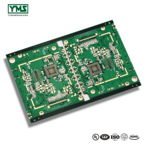
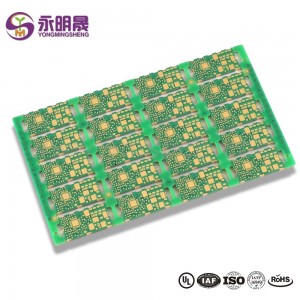
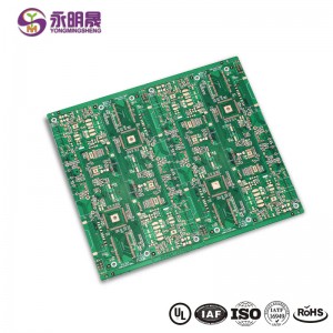
Leading Manufacturer for 2.0W/Mk pcb copper plate with low price in China
Board2.jpg)
To be the stage of realizing dreams of our employees! To build a happier, far more united and far more specialist team! To reach a mutual profit of our customers, suppliers, the society and ourselves for Leading Manufacturer for 2.0W/Mk pcb copper plate with low price in China, We welcome new and outdated clients to get in touch with us by cell phone or send us inquiries by mail for long term business relationships and accomplishing mutual results.
To be the stage of realizing dreams of our employees! To build a happier, far more united and far more specialist team! To reach a mutual profit of our customers, suppliers, the society and ourselves for , Based on our guiding principle of quality is the key to development, we continually strive to exceed our customers’ expectations. As such, we sincerely invite all interested companies to contact us for future cooperation, We welcome old and new customers to hold hands together for exploring and developing; For more information, please feel free to contact us. Thanks. Advanced equipment, strict quality control, customer-orientation service, initiative summary and improvement of defects and extensive industry experience enable us to guarantee more customer satisfaction and reputation which, in return, brings us more orders and benefits. If you are interested in any of our products and solutions, make sure you feel free to contact us. Inquiry or visit to our company are warmly welcome. We sincerely hope to start a win-win and friendly partnership with you. You can see more details in our website.
Thick copper plate basic production process:
A、The inner core plate is obtained by cutting materials, and the inner circuit is made on each inner core plate respectively through the processing of inner graph and etching. A number of copper pads are interleaved on the edge of the plate in the open area of each inner core plate to make each inner core plate.
B、The inner layer and outer layer of copper foil are pressed together by semi-curing sheet to make multi-layer production plate.
C、According to the existing technology, the thick copper plate is prepared by the post-treatment of the multilayer production plate.
You May Like:
1、What are the precautions for heavy copper PCB wiring
2、What are the specifications of heavy copper PCB
3、What are the heavy copper PCB materials
Products categories
-
China Manufacturer for Customized Printing Circ...
-
OEM China Hot Sale Fan Remote Control Pcb 12 Oz...
-

Good Quality Customized 0.5mm Thickness Green S...
-
Factory wholesale 1.1mm Printing Aluminum Subli...
-
Special Design for China Multilayer Printed Cir...
-
Wholesale Price China China 14 Layer HDI PCB Ma...


