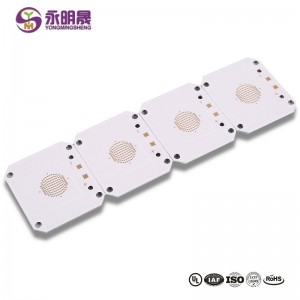
High Frequency PCBs manufacturing PTFE and FR4 Hybrid blind via| YMSPCB

What is RF & Microwave PCB ?
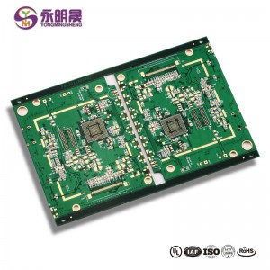
Radio frequency (RF) and microwave PCB’s are a type of PCB designed to operate on signals in the medium frequency to extremely high frequency ranges (megahertz to gigahertz). These ranges are used for communication signals in everything from mobile phones to military radars.
The materials used are advanced composites with very specific characteristics for dielectric constant (Er), loss tangent, and CTE (co-efficient of thermal expansion). These materials can be mixed in the same Stack-Up for optimal performance and economics.
In order to meet increasing demands for Microwave & RF Printed Circuit Boards for our customers all around the world, we have increased our investment over the last few years so that we have become a world class manufacturer of PCBs using high frequency laminates.
YMS Microwave & RF PCB manufacturing capabilities:
| YMS Microwave/RF PCB manufacturing capabilities overview | ||
| Feature | capabilities | |
| Layer Count | 2-14L | |
| Available Microwave/RF PCB Technology | Through hole with Aspect Ratio 16:1 | |
| buried and blind via | ||
| Mixed Dielectric Boards (PTFE+FR-4 combinations ) | ||
| Suitable Microwave/RF Materials available : PTFE, FR4, Polymide, Polyester, Ceramic | ||
| Tight Etch Tolerances on Critical RF Features:+/- .0005" standard tolerance for unplated 0.5oz copper | ||
| Multilevel cavity constructions, Copper coins and slugs, Metal Core & Metal Back, Thermally conductive laminates,Edge Plating, etc. | ||
| Thickness | 0.3mm-8mm | |
| Minimum line Width and Space | 0.075mm/0.075mm(3mil/3mil) | |
| BGA PITCH | 0.35mm | |
| Min laser Drilled Size | 0.075mm(3nil) | |
| Min mechanical Drilled Size | 0.15mm(6mil) | |
| Aspect Ratio for laser hole | 0.9:1 | |
| Aspect Ratio for through hole | 16:1 | |
| Surface Finish | Suitable Microwave/RF PCB urface finishes: Electroless Nickel, Immersion Gold, ENEPIG, Lead free HASL,Immersion Silver | |
| Via Fill Option | The via is plated and filled with either conductive or non-conductive epoxy then capped and plated over(VIPPO) | |
| Copper filled, silver filled | ||
| Laser via copper plated shut | ||
| Registration | ±4mil | |
| Solder Mask | Green, Red, Yellow, Blue, White, Black, Purple, Matte Black, Matte green.etc. | |
Learn more about YMS products
Read more news