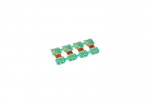
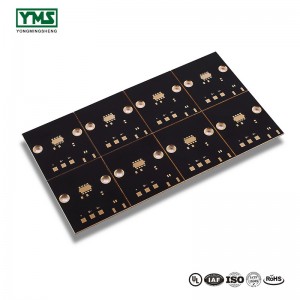
Europe style for OEM service heavy copper PCB board made by HX circuit PCB manufacturer with 15 years experience and Net 30 days Payment
Board2.jpg)
It truly is our responsibility to fulfill your requirements and successfully provide you. Your fulfillment is our best reward. We’re seeking forward in your check out for joint development for Europe style for OEM service heavy copper PCB board made by HX circuit PCB manufacturer with 15 years experience and Net 30 days Payment, And there are also many foreign friends who came for sight seeing, or entrust us to buy other stuff for them. You are most welcome to come to China, to our city and to our factory!
It truly is our responsibility to fulfill your requirements and successfully provide you. Your fulfillment is our best reward. We’re seeking forward in your check out for joint development for , Our items have national accreditation requirements for qualified, high quality products, affordable value, was welcomed by people today all over the world. Our goods will continue to enhance within the order and look forward to cooperation with you, Should any of these products be of interest to you, please letus know. We are going to be content to offer you a quotation up on receipt of your detailed needs.
Heavy Copper PCB are printed circuit boards with 3 or more ounces of finished copper in the inner and/or outer layers.
While there is no standard definition of Heavy Copper, it is generally accepted that if 3 ounces (oz) of copper or more is used on the internal and external layers of a printed circuit board, it is called a heavy copper PCB. Any circuit with a copper thickness of more than 4 oz per square foot (ft2) is also categorized as a heavy copper PCB.
The construction of a heavy copper circuit endows a board with benefits such as:
- Increased endurance to thermal strains.
- Increased current carrying capacity.
- Increased mechanical strength at connector sites and in PTH holes.
- Use of exotic materials to their full potential without circuit failure.
- Reduced product size by incorporating multiple copper weights on the same layer of circuitry .
- Heavy copper plated vias carry higher current through the board and help to transfer heat to an external heatsink.
Thick copper plate basic production process:
A、The inner core plate is obtained by cutting materials, and the inner circuit is made on each inner core plate respectively through the processing of inner graph and etching. A number of copper pads are interleaved on the edge of the plate in the open area of each inner core plate to make each inner core plate.
B、The inner layer and outer layer of copper foil are pressed together by semi-curing sheet to make multi-layer production plate.
C、According to the existing technology, the thick copper plate is prepared by the post-treatment of the multilayer production plate.
You May Like:
1、What are the precautions for heavy copper PCB wiring
2、What are the specifications of heavy copper PCB
3、What are the heavy copper PCB materials