
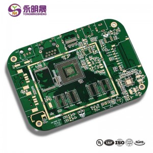
Any layer hdi pcb 12Layer Staggered Vias Immersion Gold| YMS PCB

What is HDI PCB?
HDI PCB: High density interconnect PCB, are a way of making more room on your printed circuit board to make them more efficient and allow for faster transmission. It's relatively easy for most enterprising companies that are using printed circuit boards to see how this can benefit them.
Uru nke HDI PCB
Ihe kachasị mkpa maka iji teknụzụ HDI bụ mmụba dị ukwuu na njupụta nkwakọ ngwaahịa. Oghere enwetara site na usoro egwu kachasị mma dị maka akụrụngwa. E wezụga nke ahụ, achọrọ ịbelata ohere niile ga-eme ka obere mbadamba na obere ọkwa.
Emekarị FPGA ma ọ bụ BGA dị na 1mm ma ọ bụ obere spacing. Teknụzụ HDI na-eme ka ịgbagharị na njikọ dị mfe, ọkachasị mgbe ị na-agbagharị n'etiti ntụtụ.
YMS HDI PCB n'ichepụta capa ọrụ:
| YMS HDI PCB n'ichepụta ike nnyocha | |
| Njirimara | ikike |
| Layer agụ | 4-60L |
| Nwere HDI PCB Technology | 1 + N + 1 |
| 2 + N + 2 | |
| 3 + N + 3 | |
| 4 + N + 4 | |
| 5 + N + 5 | |
| Ọ bụla oyi akwa | |
| Ọkpụrụkpụ | 0.3mm-6mm |
| Opekempe akara Obosara na Ohere | 0.05mm / 0.05mm (2mil / 2mil) |
| BGA PITCH | 0.35mm |
| Min laser gbapuru Size | 0.075mm (3nil) |
| Min n'ibu gbapuru Size | 0.15mm (6mil) |
| Akụkụ ruru maka laser onu | 0.9: 1 |
| Akụkụ Ratio maka site na oghere | 16: 1 |
| Elu rụchaa | HASL, Duru free HASL, ENIG, Imikpu Tin, OSP, ọlaọcha imikpu, mkpịsị aka mkpịsị aka, Ntinye ọla edo siri ike, ịhọrọ OSP , ENEPIG.etc. |
| Via Dejupụta Nhọrọ | The via na-plated ma jupụta ma conductive ma ọ bụ ndị na-abụghị conductive epoxy ahụ capped na plated |
| Ọla kọpa jupụtara, ọlaọcha jupụtara | |
| Laser site na ọla kọpa plated mechie | |
| Ndebanye aha | ± 4mil |
| Nkpuchi Solder | Green, Red, Yellow, Blue, White, Nwa, Purple, Matte Black, Matte green. Wdg. |
May nwere ike amasị:
1、How to identify gold on a pcb
4、The main causes of PCB board deformation and rupture
Mụtakwuo maka ngwaahịa YMS

ngwaahịa na edemede
-

HDI PCB 2 + n + 2 VIPPO High njupụta Interconnect P ...
-

SMD Ikanam ngosi ihuenyo pcb Micro ada pcb mini l ...
-

HDI PCB 3 + N + 3 Laser via ọla kọpa plated mechie Nkedo ...
-

Ikanam ngosi ihuenyo PCB HDI laser site na PAD cop ...
-

Micro site na PCB HDI PCB 8L 1 + N + 1 Via na PAD | YMSPCB
-

Wholesale Multi Layer PCB-PCB Manufacturer Chin...


