
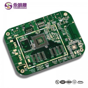
Any layer hdi pcb 12Layer Staggered Vias Immersion Gold| YMS PCB

What is HDI PCB?
Ko te HDI PCB: High density interconnect PCB, are a way of making more room on your printed circuit board to make them more efficient and allow for faster transmission. It's relatively easy for most enterprising companies that are using printed circuit boards to see how this can benefit them.
Nga painga o HDI PCB
Ko te take nui mo te whakamahi i te hangarau HDI ko te tino piki ake o te kaha tākai. Ko te waahi i whiwhihia e nga hanganga ara pai hei waatea mo nga waahanga. Ano hoki, ko nga whakaritenga o te waahi ka whakaitihia ka iti ake te rahi o te poari me te iti o nga papa.
I te nuinga o te wa e waatea ana te FPGA, te BGA ranei, me te 1mm iti ake ranei te mokowhiti. Ma te hangarau HDI e ngawari ai te nekehanga me te hononga, ina koa ka huri i waenga i nga titi.
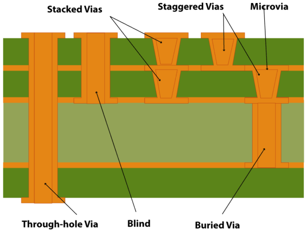
YMS HDI PCB whakahoahoa i nga hononga capa :
| YMS HDI PCB whakangao tirohanga kaha | |
| Āhuahira | āheinga |
| Kaute Papa | 4-60L |
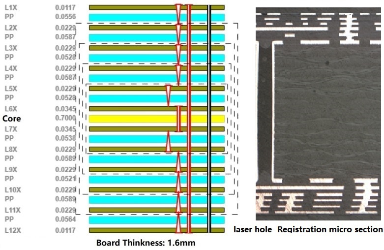
| Kei te waatea HDI PCB Hangarau | 1 + N + 1 |
| 2 + N + 2 | |
| 3 + N + 3 | |
| 4 + N + 4 | |
| 5 + N + 5 | |
| Tetahi paparanga | |
| Matotoru | 0.3mm-6mm |
| Raina Itinga Whanui me te Mokowā | 0.05mm / 0.05mm (2mil / 2mil) |
| BGA PITCH | 0.35mm |
| Min laser Te Rahi Rore | 0.075mm (3nil) |
| Te miihini Min | 0.15mm (6mil) |
| Ratio Wahanga mo te poka laser | 0.9: 1 |
| Ratio Wahanga mo te poka | 16: 1 |
| Mata Whakamutunga | HASL, Lead free HASL, ENIG, Immersion Tin, OSP, Immersion Silver, Gold Finger, Electroplating Hard Gold, Selective OSP, ENEPIG.etc. |
| Ma te Kii Whakakii | Ka whakakikihia te via ka whakakiihia ki te epoxy arataki kore-arataki ranei ka kapi ka pani |
| Kapi kapi, kapi hiriwa | |
| Taiaho ma te parahi whakakikoruatia tutakina | |
| Rehitatanga | ± 4mira |
| Mask Topi | Kakarariki, Whero, kowhai, Kahurangi, Ma, Mangu, Waiporoporo, Matte Pango, Matte matariki. |
Akene Ka Pai koe:
1、How to identify gold on a pcb
4、The main causes of PCB board deformation and rupture
6、Kei hea nga HDI PCB e whakamahia ana
Ako atu mo nga hua YMS

Products kāwai
-

Micro na PCB HDI PCB 8L 1 + N + 1 Ma runga PAD | YMSPCB
-

HDI pcb 3 + N + 3 Laser na te parahi i whakakikoruatia te Katia ...
-

Wholesale Multi Layer PCB-PCB Manufacturer Chin...
-

SMD LED mata whakaatu pcb Micro arahina pcb mini l ...
-

Whakaaturanga whakaatu rama pcb HDI laser na roto i te PAD cop ...
-

HDI Taarua Poari Porowhita 8Layer 2 Hipanga HDI PCB ...


