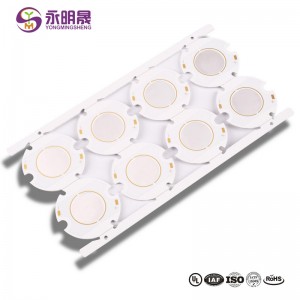
ODM Factory China Fr4 Copper Double Sided Custom PCB Boards Gold Finger for Game Machine 4 Layer PCB
Board23.jpg)
Our mission would be to grow to be an innovative provider of high-tech digital and communication devices by offering benefit added style, world-class production, and repair capabilities for ODM Factory China Fr4 Copper Double Sided Custom PCB Boards Gold Finger for Game Machine 4 Layer PCB, Never-ending improvement and striving for 0% deficiency are our two main quality policies. Should you need anything, never hesitate to get in touch with us.
Our mission would be to grow to be an innovative provider of high-tech digital and communication devices by offering benefit added style, world-class production, and repair capabilities for China Custom PCB Boards, PCB Boards Gold Finger, All the imported machines effectively control and guarantee the machining precision for the products and solutions. Besides, we have now a group of high-quality management personnels and professionals, who make the high-quality solutions and have the ability to develop new goods to expand our market home and abroad. We sincerely expect customers come for a blooming business for both of us.
Heavy Copper PCB are printed circuit boards with 3 or more ounces of finished copper in the inner and/or outer layers.
While there is no standard definition of Heavy Copper, it is generally accepted that if 3 ounces (oz) of copper or more is used on the internal and external layers of a printed circuit board, it is called a heavy copper PCB. Any circuit with a copper thickness of more than 4 oz per square foot (ft2) is also categorized as a heavy copper PCB.
The construction of a heavy copper circuit endows a board with benefits such as:
- Increased endurance to thermal strains.
- Increased current carrying capacity.
- Increased mechanical strength at connector sites and in PTH holes.
- Use of exotic materials to their full potential without circuit failure.
- Reduced product size by incorporating multiple copper weights on the same layer of circuitry .
- Heavy copper plated vias carry higher current through the board and help to transfer heat to an external heatsink.
Thick copper plate basic production process:
A、The inner core plate is obtained by cutting materials, and the inner circuit is made on each inner core plate respectively through the processing of inner graph and etching. A number of copper pads are interleaved on the edge of the plate in the open area of each inner core plate to make each inner core plate.
B、The inner layer and outer layer of copper foil are pressed together by semi-curing sheet to make multi-layer production plate.
C、According to the existing technology, the thick copper plate is prepared by the post-treatment of the multilayer production plate.
You May Like:
1、What are the precautions for heavy copper PCB wiring
2、What are the specifications of heavy copper PCB
3、What are the heavy copper PCB materials