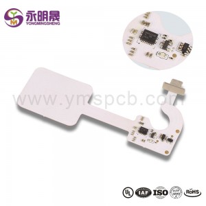
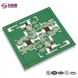
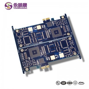
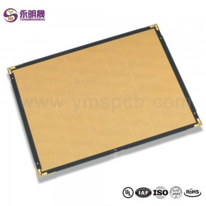
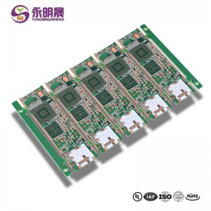
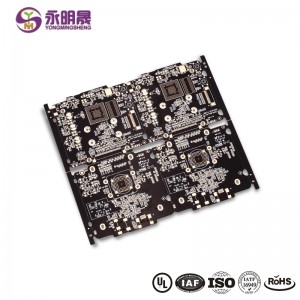
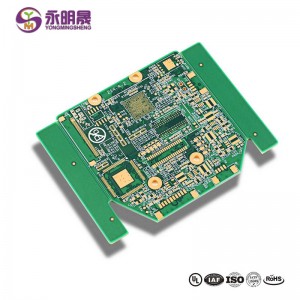
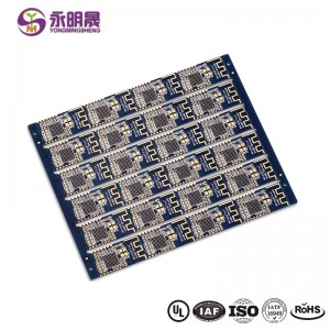
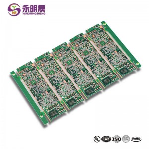
HDI printed circuit boards 8Layer 2 Step HDI Board| YMS PCB
Farashin PCB is the high-density interconnector PCB. It is a type of PCB technology that is very popular in various devices. HDI PCBs are the results of miniaturization of components and semiconductor packages because they can realize more functions on the same or less board area through some technologies.
HDI PCBs have finer lines, minor holes, and higher density than conventional PCBs, providing necessary touting solutions for the chips with many pins in mobile devices and other high-tech products.HDI PCB usually has 4,6,8 layer or even higher.
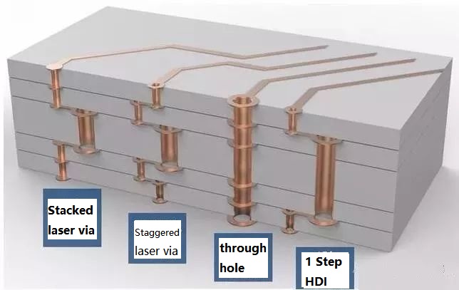
HDI design combines dense component placement and finer circuits, using less board without compromise functions. Compared to ordinary PCBs, the main difference is that HDI PCBs realize the interconnect through blind vias and buried vias instead of through holes. And HDI PCBs use laser drilling while traditional PCBs usually use mechanical drilling. The birth of the HDI PCBs brings more possibilities for portable electronic devices and more challenges for PCB manufacturers. For accommodating the trend of miniaturization and multifunction of electronics, YMS has done a lot to improve the level of equipment and staff professionalism. You can be assured to offer us the HDI designs, and we will give you a satisfactory service and HDI products.
HDI Board samar da tsari:
At present, HDI board interconnection between layer and layer is mainly the following design: Staggered holes interconnection, Cross-layer interconnection, ladder interconnection and superposition holes interconnection. Among them, the superposition holes interconnection occupy the least space. There is a research suggests that reducing the number of through holes and increasing the number of blind holes can effectively improve the wiring density. And in the superposition interconnection, the methods of electroplating and resin plug are mainly used, especially the electroplating hole filling method which has more obvious advantages like high reliability and good conduction performance. Therefore, superposition interconnection is the most widely used design method for blind holes design. The process of stacking between layers is as follows: first blind hole is made, then second blind hole is made after lamination, then multi-blind hole is made according to this method, and the interconnection between layers is realized by electroplating hole filling method.
A kan dukan, da samar da tsari na HDI farantin ne hadaddun, wanda bukatar a kammala bayan sau da yawa na samar na dogon lokaci. Yana ba kawai high bukatun ga daidaito da kuma shrinkage iko da kowane Layer, amma kuma babban matsayin da kayan, kayan aiki, yanayi da kuma fasaha ma'aikata.
YMS HDI PCB manufacturing capabilities:
| YMS HDI PCB damar duba abubuwa | |
| Fasali | damar |
| Countididdigar Layer | 4-60L |
| Akwai HDI PCB Fasaha | 1 + N + 1 |
| 2 + N + 2 | |
| 3 + N + 3 | |
| 4 + N + 4 | |
| 5 + N + 5 | |
| Duk wani Layer | |
| Kauri | 0.3mm-6mm |
| Ananan Layin Faɗi da Sarari | 0.05mm / 0.05mm (2mil / 2mil) |
| FITAR BGA | 0.35mm |
| Min Laser Harshen Girman | 0.075mm (3nil) |
| Min Girman Hannun injina | 0.15mm (6mil) |
| Ra'ayin ƙasa don ramin laser | 0.9: 1 |
| Ra'ayin ƙasa don rami | 16: 1 |
| Gama Gama | HASL, Jagora kyauta HASL, ENIG, Nitsar da Tin, OSP, Azurfar Nutsewa, Yatsan Zinare, Gyara Zinariya Mai Wuya, Mai Zaba OSP , ENEPIG.etc. |
| Ta Hanyar Cika zaɓi | An lika abin da ke ciki kuma an cika shi da mai sarrafawa ko wanda ba zai iya sarrafawa ba sannan a rufe shi |
| An cika tagulla, an cika azurfa | |
| Laser ta hanyar rufe farin ƙarfe | |
| Rijista | ± 4mil |
| Masassarar Solder | Kore, Ja, Rawaya, Shuɗi, Fari, Baƙi, Mai Tsara, Matta Baki, Matte kore. Da dai sauransu. |
Ƙara koyo game da samfuran YMS


What is HDI material?
FR4 Fiberglass board or ceramic board
Are printed circuit boards still used?
Yes,the Printed circuit board(PCB) is the foundation of electronic equipment, and it can be found in every electronic device in today ’s world
What is the major disadvantage of printed circuit boards?
1.single use 2.environmental pollution 3.high cost
Is there gold in printed circuit boards?
yes,there is


