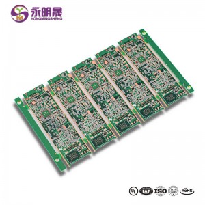
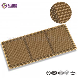
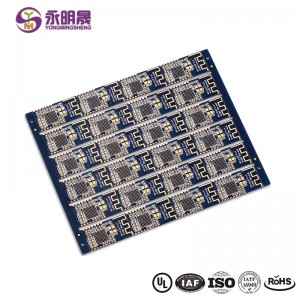
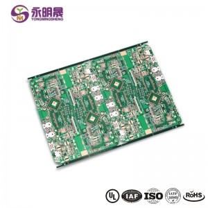
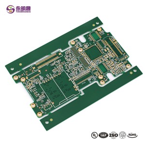
HDI printed circuit boards 8Layer 2 Step HDI Board| YMS PCB
HDI پي سي بي is the high-density interconnector PCB. It is a type of PCB technology that is very popular in various devices. HDI PCBs are the results of miniaturization of components and semiconductor packages because they can realize more functions on the same or less board area through some technologies.
HDI PCBs have finer lines, minor holes, and higher density than conventional PCBs, providing necessary touting solutions for the chips with many pins in mobile devices and other high-tech products.HDI PCB usually has 4,6,8 layer or even higher.
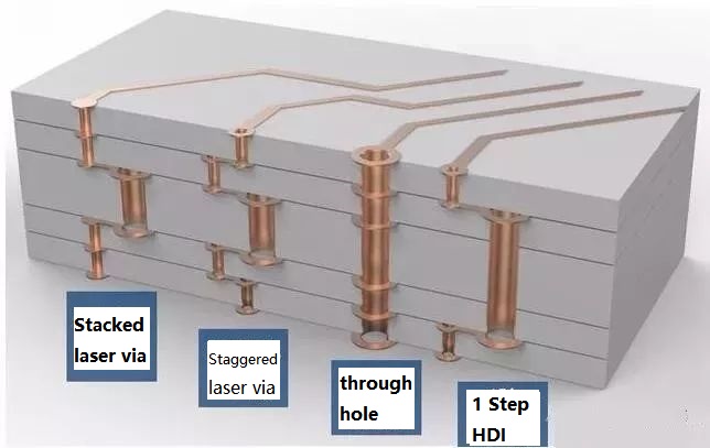
HDI design combines dense component placement and finer circuits, using less board without compromise functions. Compared to ordinary PCBs, the main difference is that HDI PCBs realize the interconnect through blind vias and buried vias instead of through holes. And HDI PCBs use laser drilling while traditional PCBs usually use mechanical drilling. The birth of the HDI PCBs brings more possibilities for portable electronic devices and more challenges for PCB manufacturers. For accommodating the trend of miniaturization and multifunction of electronics, YMS has done a lot to improve the level of equipment and staff professionalism. You can be assured to offer us the HDI designs, and we will give you a satisfactory service and HDI products.
HDI بورڊ جي پيداوار عمل:
At present, HDI board interconnection between layer and layer is mainly the following design: Staggered holes interconnection, Cross-layer interconnection, ladder interconnection and superposition holes interconnection. Among them, the superposition holes interconnection occupy the least space. There is a research suggests that reducing the number of through holes and increasing the number of blind holes can effectively improve the wiring density. And in the superposition interconnection, the methods of electroplating and resin plug are mainly used, especially the electroplating hole filling method which has more obvious advantages like high reliability and good conduction performance. Therefore, superposition interconnection is the most widely used design method for blind holes design. The process of stacking between layers is as follows: first blind hole is made, then second blind hole is made after lamination, then multi-blind hole is made according to this method, and the interconnection between layers is realized by electroplating hole filling method.
سڄي تي، HDI پتل جي پيداوار جي عمل ۾ هڪ ڊگهي وقت تائين جي پيداوار جا ڪيترا ئي ڀيرا کان پوء مڪمل ٿيڻ سان واسطو رکي ٿو جنهن جي ڳتيل آهي. اهو هر پرت جي درستگي ۽ shrinkage قبضي لاء نه رڳو اعلي ضرورتن، پر پڻ ۽ مواد ۾ اعلي معيار، سامان، ماحول فني اهلڪار آهي.
YMS HDI PCB manufacturing capabilities:
| YMS HDI پي سي بي ٺاھڻ جي صلاحيت جو جائزو | |
| خصوصيت | صلاحيتون |
| پرت جي ڳڻپ | 4-60L |
| دستياب HDI پي سي بي ٽيڪنالاجي | 1 + اين + 1 |
| 2 + اين + 2 | |
| 3 + اين + 3 | |
| 4 + اين + 4 | |
| 5 + اين + 5 | |
| ڪا به پرت | |
| ٿولهه | 0.3mm-6mm |
| گھٽ ۾ گھٽ لڪير جي ويڪرائي ۽ جاءِ | 0.05mm / 0.05mm (2mil / 2mil) |
| بيگا پيچو | 0.35 ايم ايم |
| منٽ ليزر سوراخ ٿيل سائيز | 0.075 ميلي (3 نيل) |
| گھٽ ميڪاني ڊريل سائيز | 0.15 ملي ميٽر (6 ميل) |
| ليزر سوراخ جي جهلڪ تناسب | 0.9: 1 |
| سوراخ جي ذريعي جيتري تناسب | 16: 1 |
| مٿاڇري ختم | HASL ، Lead Free HASL ، ENIG ، Immersion Tin ، OSP ، Immersion Silver ، Gold Finger ، Electroplating Hard Gold ، Selective OSP , ENEPIG.etc. |
| في آپشن ذريعي | وچ ۾ پليو ويو آهي ۽ يا ٻيو ڪو نان ڪوليڪوڪ يا غير ڪنٽليوٽ ايوپوڪس سان ڀريو ويو آهي |
| ٽامي ڀريل ، چاندي ڀريل | |
| ليزر ذريعي ڪاپر پلٽيڊ بند | |
| رجسٽريشن | ± 4مل |
| سولڊر ماسڪ | سائو ، ڳاڙھو ، پيلو ، نيرو ، اڇو ، ڪارو ، جامني ، مٽي ڪارو ، مٽي سائو وغيره. |
و Learnيڪ سکو YMS پروڊڪٽس بابت


What is HDI material?
FR4 Fiberglass board or ceramic board
Are printed circuit boards still used?
Yes,the Printed circuit board(PCB) is the foundation of electronic equipment, and it can be found in every electronic device in today ’s world
What is the major disadvantage of printed circuit boards?
1.single use 2.environmental pollution 3.high cost
Is there gold in printed circuit boards?
yes,there is


