
Double Layer PCB Countersink Halogen Free Material| YMS PCB

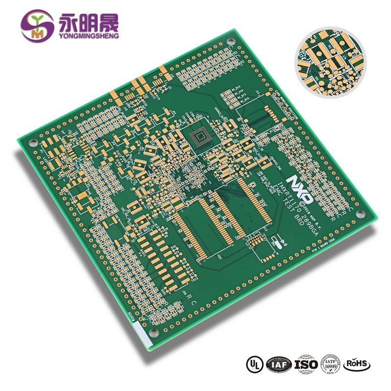
China two layer Fr4 PCB is one of the most popular types of PCBs because they make manufacturers to fabricate more complex circuits, which can benefit uses in higher technology applications and electronics. There is an abundance of applications and electronics which double sided PCBs can be used in electronics such as:LED lighting systems、Consumer Electronics.
What is the difference between a Countersink and a Counterbore?

YMS Normal PCB manufacturing capabilities:
| YMS Normal PCB manufacturing capabilities overview | ||
| Feature | capabilities | |
| Layer Count | 1-60L | |
| Available Normal PCB Technology | Through hole with Aspect Ratio 16:1 | |
| buried and blind via | ||
| Hybrid | High Frequency Material such as RO4350B and FR4 Mix etc. | |
| High Speed Material such as M7NE and FR4 Mix etc. | ||
| Material | CEM- | CEM-1;CEM-2;CEM-4;CEM-5.etc |
| FR4 | EM827, 370HR, S1000-2, IT180A, IT158, S1000 / S1155, R1566W, EM285, TU862HF,NP170G etc. | |
| High Speed | Megtron6, Megtron4, Megtron7,TU872SLK, FR408HR,N4000-13 Series,MW4000,MW2000,TU933 etc. | |
| High Frequency | Ro3003, Ro3006, Ro4350B, Ro4360G2, Ro4835, CLTE, Genclad, RF35, FastRise27 etc. | |
| Others | Polyimide, Tk, LCP, BT, C-ply, Fradflex, Omega , ZBC2000,PEEK,PTFE,ceramic-based etc. | |
| Thickness | 0.3mm-8mm | |
| Max.copper Thickness | 10OZ | |
| Minimum line Width and Space | 0.05mm/0.05mm(2mil/2mil) | |
| BGA PITCH | 0.35mm | |
| Min mechanical Drilled Size | 0.15mm(6mil) | |
| Aspect Ratio for through hole | 16:1 | |
| Surface Finish | HASL, Lead free HASL,ENIG,Immersion Tin, OSP, Immersion Silver, Gold Finger, Electroplating Hard Gold, Selective OSP,ENEPIG.etc. | |
| Via Fill Option | The via is plated and filled with either conductive or non-conductive epoxy then capped and plated over(VIPPO) | |
| Copper filled, silver filled | ||
| Registration | ±4mil | |
| Solder Mask | Green, Red, Yellow, Blue, White, Black, Purple, Matte Black, Matte green.etc. | |
Learn more about YMS products

What is double layer PCB?
A two layer PCB is a type of PCB which has conductive copper layers on both sides of the board.
What are double sided PCBs used for?
Fiber optics;Car dashboards;GPS systems.
Can a PCB have multi layers?
yes, the layers can be more higher per stackup.
What is difference between single sided and double sided PCB?
Double-sided PCBs are the same as single-sided PCBs, but the difference is they have two sided traces with a top and bottom layer.
Write your message here and send it to us

Board21-300x300.jpg)
