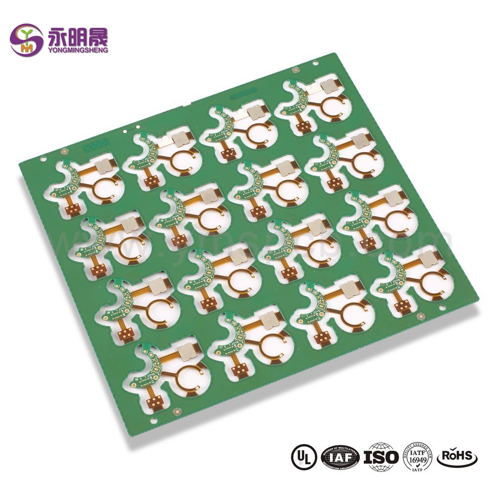
Double sided pcb Normal pcb Lead free HASL Counterbore Manufacturer | YMS PCB
HAL(Lead Free), the full name is Hot Air leveling with Lead Free. Compared with HASL, the main difference for HAL(Lead Free) is the element of material which do not contain Lead(Pb), so it’s RoHS Compliant and it’s much more popular and widely used in gweithgynhyrchu PCB .
HAL(Lead Free) requires higher run temperatures for lead free solder and longer contact time, the production cost for HAL(Lead Free) is slightly higher than HASL(Tin/Lead).
The manufacturing process of HAL(Lead Free) is similar to HASL(Tin/Lead), the circuit boards will be submersed in molten solder(Lead Free). This solder will cover all the exposed copper surfaces. Upon retraction from the solder, high pressure hot air is blown over the surface through air knives, this levels the solder deposit and removes the excess solder from the surface of printed circuit boards.
Cyflwyniad y Bwrdd Cylchdaith Argraffedig
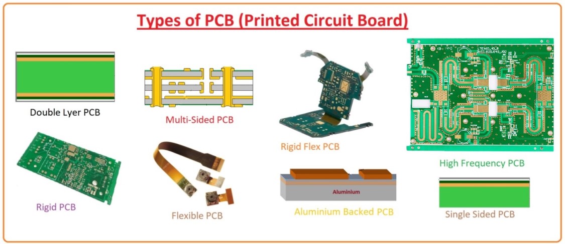
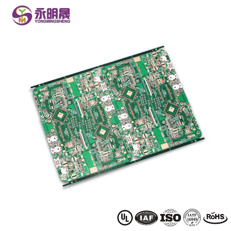
Bwrdd Cylchdaith Argraffedig Arferol: Most PCBs for simple electronics are simple and composed of only a single layer. More sophisticated hardware such as computer graphics cards or motherboards can have 2 or multiple layers, sometimes up to twelve.
A printed circuit board (PCB) mechanically supports and electrically connects electrical or electronic components using conductive tracks, pads and other features etched from one or more sheet layers of copper laminated onto and/or between sheet layers of a non-conductive substrate. Components are generally soldered onto the PCB to both electrically connect and mechanically fasten them to it.PCBs can be single-sided (one copper layer), double-sided (two copper layers on both sides of one substrate layer), or multi-layer (outer and inner layers of copper, alternating with layers of substrate). Multi-layer PCBs allow for much higher component density, because circuit traces on the inner layers would otherwise take up surface space between components. The rise in popularity of multilayer PCBs with more than two, and especially with more than four, copper planes was concurrent with the adoption of surface mount technology.
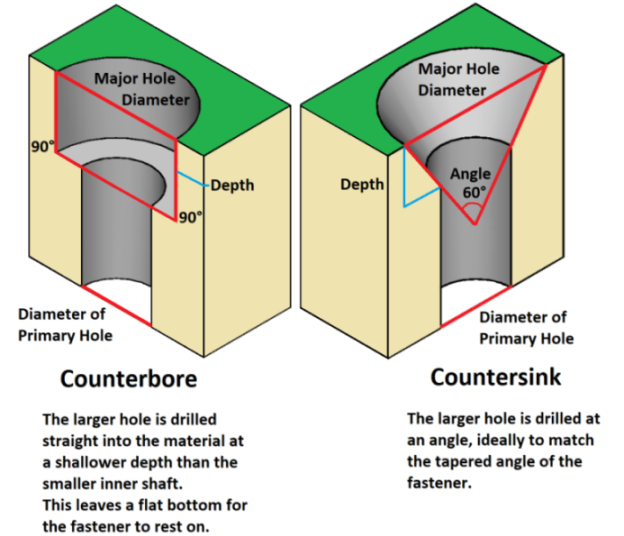
What is the difference between a Countersink and a Counterbore?
YMS Galluoedd gweithgynhyrchu PCB arferol:
| YMS Trosolwg galluoedd gweithgynhyrchu PCB arferol | ||
| Nodwedd | galluoedd | |
| Cyfrif Haen | 1-60L | |
| Technoleg PCB Arferol Ar Gael | Trwy dwll gyda Chymhareb Agwedd 16: 1 | |
| claddedig a dall trwy | ||
| Hybrid | Deunydd Amledd Uchel fel RO4350B a FR4 Mix ac ati. | |
| Deunydd Cyflymder Uchel fel M7NE a FR4 Mix ac ati. | ||
| Deunydd | CEM- | CEM-1; CEM-2 ; CEM-4 ; CEM-5.etc |
| FR4 | EM827, 370HR, S1000-2, IT180A, IT158, S1000 / S1155, R1566W, EM285, TU862HF, NP170G ac ati. | |
| Cyflymder uchel | Megtron6, Megtron4, Megtron7, TU872SLK, FR408HR, Cyfres N4000-13, MW4000, MW2000, TU933 ac ati. | |
| Amledd uchel | Ro3003, Ro3006, Ro4350B, Ro4360G2, Ro4835, CLTE, Genclad, RF35, FastRise27 ac ati. | |
| Eraill | Polyimide, Tk, LCP, BT, C-ply, Fradflex, Omega, ZBC2000, PEEK, PTFE, yn seiliedig ar serameg ac ati. | |
| Trwch | 0.3mm-8mm | |
| Trwch Max.copper | 10OZ | |
| Lled a Gofod Isafswm y llinell | 0.05mm / 0.05mm (2mil / 2mil) | |
| BGA PITCH | 0.35mm | |
| Maint Drilio Min mecanyddol | 0.15mm (6mil) | |
| Cymhareb Agwedd ar gyfer twll drwodd | 16 : 1 | |
| Gorffen Arwyneb | HASL, HASL di-blwm, ENIG, Tun Trochi, OSP, Arian Trochi, Bys Aur, Aur Caled Electroplatio, OSP Dewisol , ENEPIG.etc. | |
| Trwy Opsiwn Llenwi | Mae'r via yn cael ei blatio a'i lenwi â naill ai epocsi dargludol neu an-ddargludol yna wedi'i gapio a'i blatio drosodd (VIPPO) | |
| Copr wedi'i lenwi, wedi'i lenwi ag arian | ||
| Cofrestru | ± 4mil | |
| Mwgwd solder | Gwyrdd, Coch, Melyn, Glas, Gwyn, Du, Porffor, Du Matte, Matte green.etc. | |
Efallai yr hoffech:
1, Crynodeb o faterion sydd angen sylw yn y weldio bwrdd cylched
3, Beth yw PCB
4、Beth yw profion bwrdd noeth?
Dysgu mwy am gynhyrchion YMS


