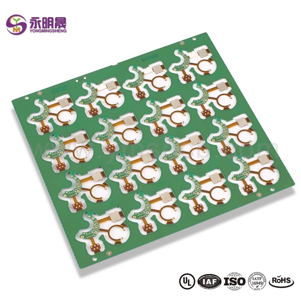
Double sided pcb Normal pcb Lead free HASL Counterbore Manufacturer | YMS PCB
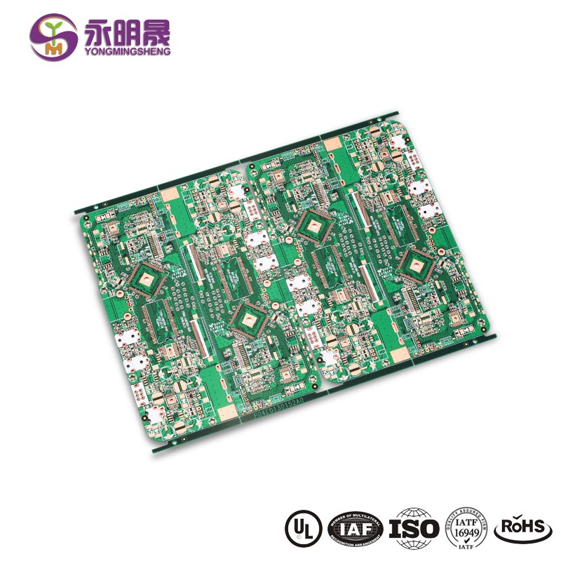
HAL(Lead Free), the full name is Hot Air leveling with Lead Free. Compared with HASL, the main difference for HAL(Lead Free) is the element of material which do not contain Lead(Pb), so it’s RoHS Compliant and it’s much more popular and widely used in PCB angitu te hanga .
HAL(Lead Free) requires higher run temperatures for lead free solder and longer contact time, the production cost for HAL(Lead Free) is slightly higher than HASL(Tin/Lead).
The manufacturing process of HAL(Lead Free) is similar to HASL(Tin/Lead), the circuit boards will be submersed in molten solder(Lead Free). This solder will cover all the exposed copper surfaces. Upon retraction from the solder, high pressure hot air is blown over the surface through air knives, this levels the solder deposit and removes the excess solder from the surface of printed circuit boards.
Panui a te Poari Porowhita Panui
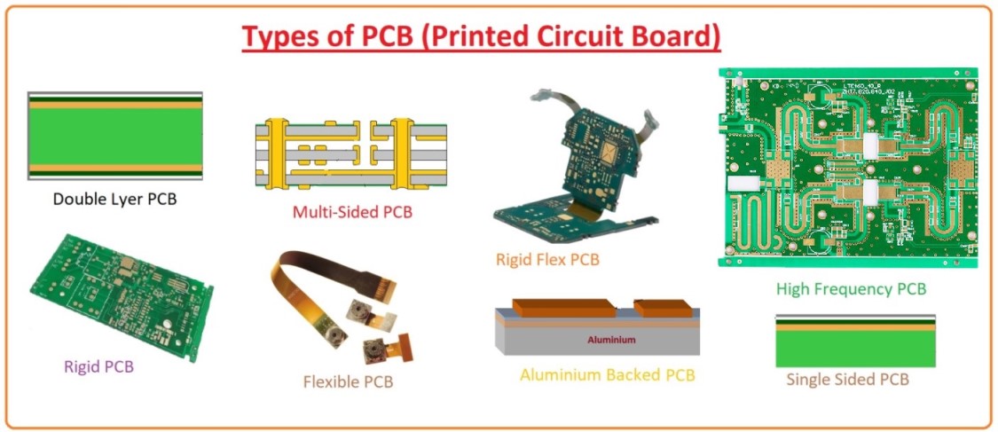
Poari Takiwa Taa Punoa: Most PCBs for simple electronics are simple and composed of only a single layer. More sophisticated hardware such as computer graphics cards or motherboards can have 2 or multiple layers, sometimes up to twelve.
A printed circuit board (PCB) mechanically supports and electrically connects electrical or electronic components using conductive tracks, pads and other features etched from one or more sheet layers of copper laminated onto and/or between sheet layers of a non-conductive substrate. Components are generally soldered onto the PCB to both electrically connect and mechanically fasten them to it.PCBs can be single-sided (one copper layer), double-sided (two copper layers on both sides of one substrate layer), or multi-layer (outer and inner layers of copper, alternating with layers of substrate). Multi-layer PCBs allow for much higher component density, because circuit traces on the inner layers would otherwise take up surface space between components. The rise in popularity of multilayer PCBs with more than two, and especially with more than four, copper planes was concurrent with the adoption of surface mount technology.
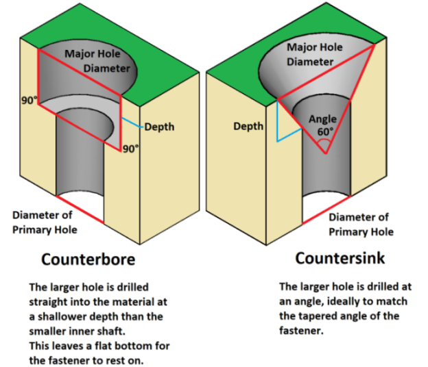
What is the difference between a Countersink and a Counterbore?
YMS Nga mahi hanga PCB noa:
| YMS Ma te PCB angitu te hanga tirohanga tirohanga | ||
| Āhuahira | āheinga | |
| Kaute Papa | 1-60L | |
| Wātea Hangarau PCB Pūnoa | Na roto i te poka me te Ratio Ahuatanga 16: 1 | |
| tanumia ka matapo via | ||
| Ranu | Rauemi Auautanga Rite penei i te RO4350B me te FR4 Mix etc. | |
| Rauemi Tere Rawa penei i te M7NE me te FR4 Mix etc. | ||
| Rauemi | CEM- | CEM-1; CEM-2 ; CEM-4 ; CEM-5.etc |
| FR4 | EM827, 370HR, S1000-2, IT180A, IT158, S1000 / S1155, R1566W, EM285, TU862HF, NP170G etc. | |
| tere High | Megtron6, Megtron4, Megtron7, TU872SLK, FR408HR, N4000-13 Series, MW4000, MW2000, TU933 etc. | |
| Auautanga High | Ro3003, Ro3006, Ro4350B, Ro4360G2, Ro4835, CLTE, Genclad, RF35, FastRise27 etc. | |
| Etahi | Polyimide, Tk, LCP, BT, C-ply, Fradflex, Omega, ZBC2000, PEEK, PTFE, te papa-uku etc. | |
| Matotoru | 0.3mm-8mm | |
| Max.copper Matotoru | 10OZ | |
| Raina Itinga Whanui me te Mokowā | 0.05mm / 0.05mm (2mil / 2mil) | |
| BGA PITCH | 0.35mm | |
| Te miihini Min | 0.15mm (6mil) | |
| Ratio Wahanga mo te poka | 16 : 1 | |
| Mata Whakamutunga | HASL, Lead free HASL, ENIG, Immersion Tin, OSP, Immersion Silver, Gold Finger, Electroplating Hard Gold, Selective OSP, ENEPIG.etc. | |
| Ma te Kii Whakakii | Ka whakakikihia te via ka whakakiihia ki te epoxy arataki kore-arataki ranei ka kapi ka whakakikihia (VIPPO) | |
| Kapi kapi, kapi hiriwa | ||
| Rehitatanga | ± 4mira | |
| Mask Topi | Kakarariki, Whero, kowhai, Kahurangi, Ma, Mangu, Waiporoporo, Matte Pango, Matte matariki. | |
Akene Ka Pai koe:
1, Summary of matters needing attention in circuit board welding
3, What is PCB
4、He aha te whakamatautau poari tahanga?
5. He aha te hoahoa PCB auau teitei
Ako atu mo nga hua YMS


