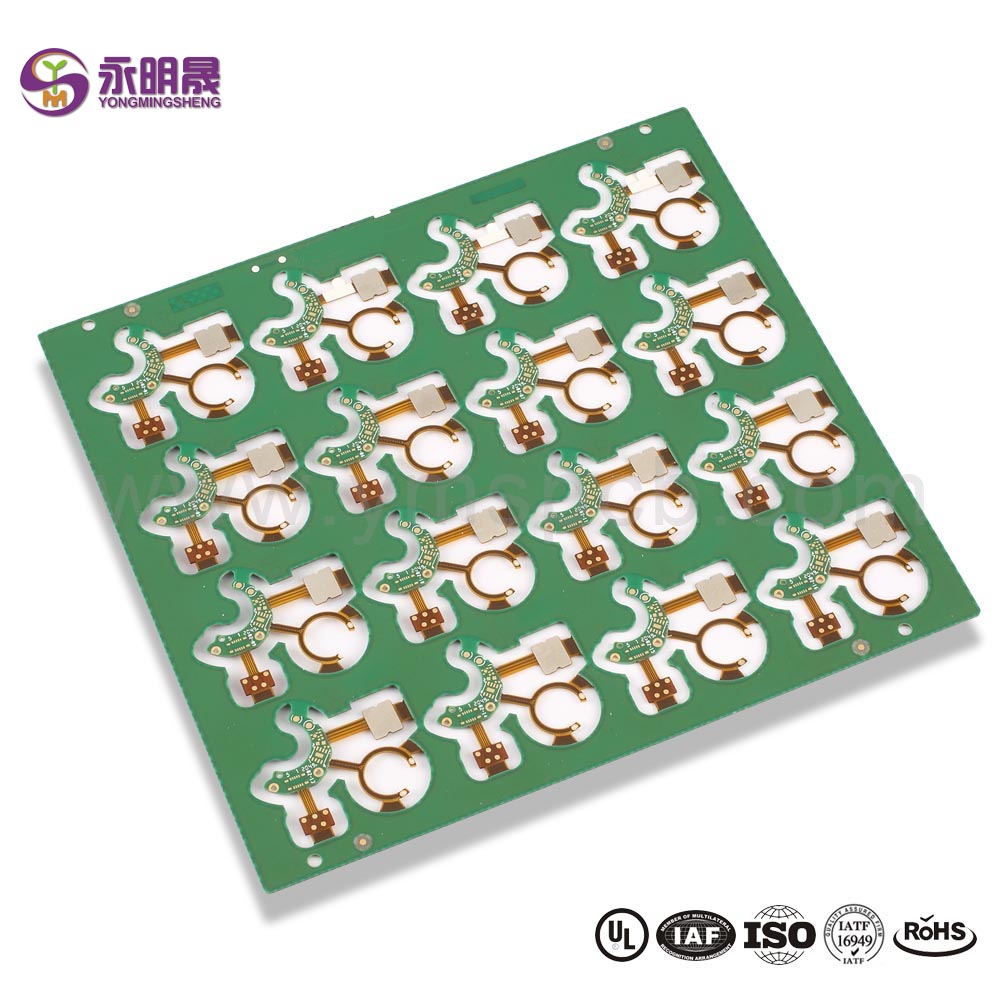
Double sided pcb Normal pcb Lead free HASL Counterbore Manufacturer | YMS PCB
HAL(Lead Free), the full name is Hot Air leveling with Lead Free. Compared with HASL, the main difference for HAL(Lead Free) is the element of material which do not contain Lead(Pb), so it’s RoHS Compliant and it’s much more popular and widely used in nrụpụta .
HAL(Lead Free) requires higher run temperatures for lead free solder and longer contact time, the production cost for HAL(Lead Free) is slightly higher than HASL(Tin/Lead).
The manufacturing process of HAL(Lead Free) is similar to HASL(Tin/Lead), the circuit boards will be submersed in molten solder(Lead Free). This solder will cover all the exposed copper surfaces. Upon retraction from the solder, high pressure hot air is blown over the surface through air knives, this levels the solder deposit and removes the excess solder from the surface of printed circuit boards.
E Bipụtara Circuit Board Okwu Mmalite
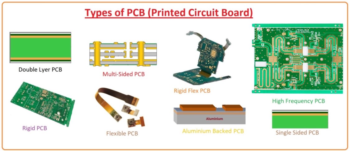
Bọdụ sekit a na-ebipụta nke ọma: Most PCBs for simple electronics are simple and composed of only a single layer. More sophisticated hardware such as computer graphics cards or motherboards can have 2 or multiple layers, sometimes up to twelve.
A printed circuit board (PCB) mechanically supports and electrically connects electrical or electronic components using conductive tracks, pads and other features etched from one or more sheet layers of copper laminated onto and/or between sheet layers of a non-conductive substrate. Components are generally soldered onto the PCB to both electrically connect and mechanically fasten them to it.PCBs can be single-sided (one copper layer), double-sided (two copper layers on both sides of one substrate layer), or multi-layer (outer and inner layers of copper, alternating with layers of substrate). Multi-layer PCBs allow for much higher component density, because circuit traces on the inner layers would otherwise take up surface space between components. The rise in popularity of multilayer PCBs with more than two, and especially with more than four, copper planes was concurrent with the adoption of surface mount technology.
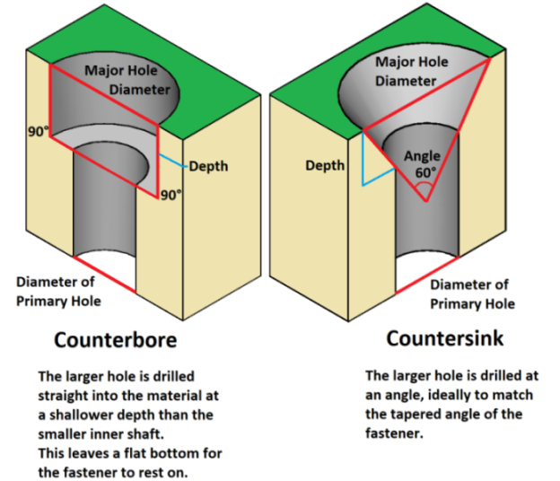
What is the difference between a Countersink and a Counterbore?
YMS Nkịtị PCB n'ichepụta ike:
| YMS Nkịtị PCB n'ichepụta ike nnyocha | ||
| Njirimara | ikike | |
| Layer agụ | 1-60L | |
| Dị Nkịtị PCB Technology | Site na oghere na akụkụ 16: 1 | |
| lie ma kpuo ìsì via | ||
| Ngwakọ | Nnukwu ihe dị ka RO4350B na FR4 Mix wdg. | |
| Ihe di elu di ka M7NE na FR4 Mix wdg. | ||
| Ihe onwunwe | CEM- | CEM-1; CEM-2 ; CEM-4 ; CEM-5.etc |
| FR4 | EM827, 370HR, S1000-2, IT180A, IT158, S1000 / S1155, R1566W, EM285, TU862HF, NP170G wdg. | |
| Oke ọsọ | Megtron6, Megtron4, Megtron7, TU872SLK, FR408HR, N4000-13 Series, MW4000, MW2000, TU933 wdg. | |
| Nnukwu Frequency | Ro3003, Ro3006, Ro4350B, Ro4360G2, Ro4835, CLTE, Genclad, RF35, FastRise27 wdg. | |
| Ndị ọzọ | Polyimide, Tk, LCP, BT, C-ply, Fradflex, Omega, ZBC2000, pee, ptfe, seramiiki dabeere wdg. | |
| Ọkpụrụkpụ | 0.3mm-8mm | |
| Max.copper ọkpụrụkpụ | 10ỌZ | |
| Opekempe akara Obosara na Ohere | 0.05mm / 0.05mm (2mil / 2mil) | |
| BGA PITCH | 0.35mm | |
| Min n'ibu gbapuru Size | 0.15mm (6mil) | |
| Akụkụ Ratio maka site na oghere | 16 : 1 | |
| Elu rụchaa | HASL, Duru free HASL, ENIG, Imikpu Tin, OSP, ọlaọcha imikpu, mkpịsị aka mkpịsị aka, Ntinye ọla edo siri ike, ịhọrọ OSP , ENEPIG.etc. | |
| Via Dejupụta Nhọrọ | The via na-plated ma jupụta ma conductive ma ọ bụ ndị na-abụghị conductive epoxy ahụ capped na plated n'elu (VIPPO) | |
| Ọla kọpa jupụtara, ọlaọcha jupụtara | ||
| Ndebanye aha | ± 4mil | |
| Nkpuchi Solder | Green, Red, Yellow, Blue, White, Nwa, Purple, Matte Black, Matte green. Wdg. | |
May nwere ike amasị:
1. Summary of matters needing attention in circuit board welding
3, What is PCB
5. Gịnị bụ elu ugboro PCB imewe
Mụtakwuo maka ngwaahịa YMS


