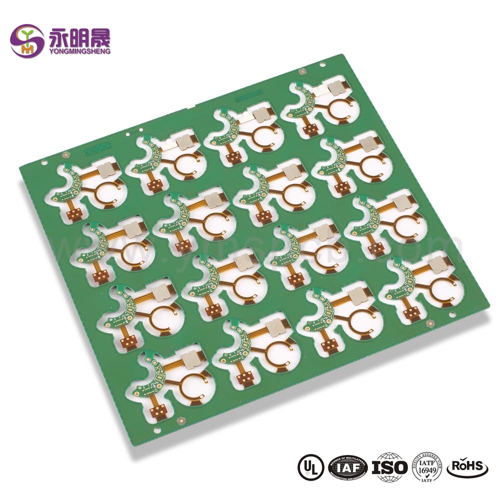
Double sided pcb Normal pcb Lead free HASL Counterbore Manufacturer | YMS PCB
HAL(Lead Free), the full name is Hot Air leveling with Lead Free. Compared with HASL, the main difference for HAL(Lead Free) is the element of material which do not contain Lead(Pb), so it’s RoHS Compliant and it’s much more popular and widely used in utengenezaji wa PCB ya .
HAL(Lead Free) requires higher run temperatures for lead free solder and longer contact time, the production cost for HAL(Lead Free) is slightly higher than HASL(Tin/Lead).
The manufacturing process of HAL(Lead Free) is similar to HASL(Tin/Lead), the circuit boards will be submersed in molten solder(Lead Free). This solder will cover all the exposed copper surfaces. Upon retraction from the solder, high pressure hot air is blown over the surface through air knives, this levels the solder deposit and removes the excess solder from the surface of printed circuit boards.
Kuchapishwa kwa Bodi ya Mzunguko
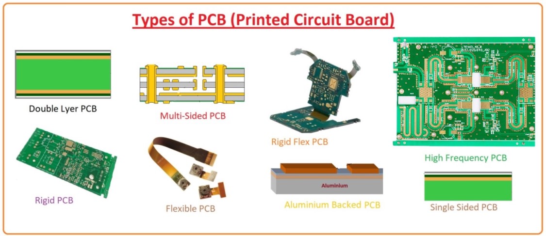
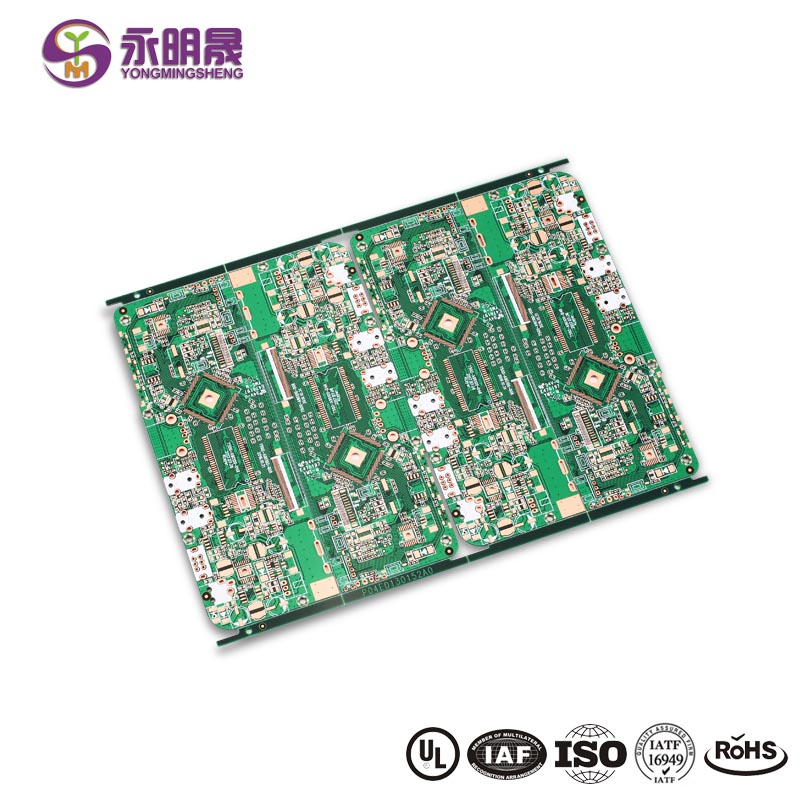
Bodi ya Mzunguko ya Kawaida Iliyochapishwa: Most PCBs for simple electronics are simple and composed of only a single layer. More sophisticated hardware such as computer graphics cards or motherboards can have 2 or multiple layers, sometimes up to twelve.
A printed circuit board (PCB) mechanically supports and electrically connects electrical or electronic components using conductive tracks, pads and other features etched from one or more sheet layers of copper laminated onto and/or between sheet layers of a non-conductive substrate. Components are generally soldered onto the PCB to both electrically connect and mechanically fasten them to it.PCBs can be single-sided (one copper layer), double-sided (two copper layers on both sides of one substrate layer), or multi-layer (outer and inner layers of copper, alternating with layers of substrate). Multi-layer PCBs allow for much higher component density, because circuit traces on the inner layers would otherwise take up surface space between components. The rise in popularity of multilayer PCBs with more than two, and especially with more than four, copper planes was concurrent with the adoption of surface mount technology.
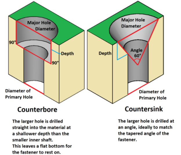
What is the difference between a Countersink and a Counterbore?
Uwezo wa utengenezaji wa PCB wa kawaida wa YMS:
| Maelezo ya jumla ya uwezo wa utengenezaji wa PCB ya YMS | ||
| Makala | uwezo | |
| Hesabu ya Tabaka | 1-60L | |
| Inapatikana Teknolojia ya Kawaida ya PCB | Kupitia shimo na Uwiano wa Vipengele 16: 1 | |
| kuzikwa na kipofu kupitia | ||
| Mseto | Nyenzo za Masafa ya Juu kama vile RO4350B na Mchanganyiko wa FR4 nk. | |
| Vifaa vya kasi kama vile M7NE na FR4 Changanya nk. | ||
| Nyenzo | CEM- | CEM-1; CEM-2, CEM-4, CEM-5. nk |
| FR4 | EM827, 370HR, S1000-2, IT180A, IT158, S1000 / S1155, R1566W, EM285, TU862HF, NP170G nk. | |
| Kasi kubwa | Megtron6, Megtron4, Megtron7, TU872SLK, FR408HR, N4000-13 Series, MW4000, MW2000, TU933 nk. | |
| high Frequency | Ro3003, Ro3006, Ro4350B, Ro4360G2, Ro4835, CLTE, Genclad, RF35, FastRise27 nk. | |
| Wengine | Polyimide, Tk, LCP, BT, C-ply, Fradflex, Omega, ZBC2000, PEEK, PTFE, msingi wa kauri nk. | |
| Unene | 0.3mm-8mm | |
| Unene wa juu wa shaba | 10OZ | |
| Kima cha chini cha upana na nafasi | 0.05mm / 0.05mm (2mil / 2mil) | |
| BGA PITCH | 0.35 mm | |
| Ukubwa mdogo wa mitambo | 0.15mm (6mil) | |
| Uwiano wa vipengele kwa kupitia shimo | 16: 1 | |
| Kumaliza uso | HASL, Kiongozi wa bure HASL, ENIG, Bati ya kuzamisha, OSP, Fedha ya Kuzamisha, Kidole cha Dhahabu, Electrlating Hard Hard, OSP Selective, ENEPIG.etc. | |
| Kupitia Chaguo la Kujaza | Njia hiyo imefunikwa na kujazwa na epoxy inayoweza kusonga au isiyo ya kushughulikia kisha imefungwa na kufunikwa (VIPPO) | |
| Shaba imejazwa, fedha imejazwa | ||
| Usajili | ± 4mil | |
| Mask ya Solder | Kijani, Nyekundu, Njano, Bluu, Nyeupe, Nyeusi, Zambarau, Matte Nyeusi, Matte kijani n.k. | |
Unaweza kama:
1, Muhtasari wa masuala wanaohitaji tahadhari katika mzunguko bodi kulehemu
3, nini PCB
4、Je! Upimaji wa bodi wazi ni nini?
5. Ubunifu wa PCB wa masafa ya juu ni nini
Jifunze zaidi kuhusu bidhaa za YMS


