
HDI pcb leha e le efe lera hdi pcb lebelo le phahameng la ho kenya tlhahlobo ea tahlehelo enepig | ETSANG

HDI PCB ke eng
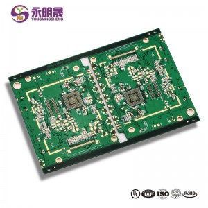
HDI PCB: High density interconnect PCB, are a way of making more room on your printed circuit board to make them more efficient and allow for faster transmission. It's relatively easy for most enterprising companies that are using printed circuit boards to see how this can benefit them.
Melemo ea HDI PCB
Lebaka le tloaelehileng haholo la ho sebelisa theknoloji ea HDI ke keketseho e kholo ea bongata ba liphutheloana. Sebaka se fumanoeng ke meaho e metle haholo sea fumaneha bakeng sa likarolo. Ntle le moo, litlhoko tsa sebaka se felletseng li tla fella ka boholo ba boto e nyane le likarolo tse fokolang.
Hangata FPGA kapa BGA li fumaneha ka sekhahla sa 1mm kapa ka tlase. Theknoloji ea HDI e etsa hore ho tsamaisoa habonolo le khokahano ho be bonolo, haholo ha ho tsamaisoa lipakeng tsa lithakhisa.
YMS HDI PCB e etsa capa :
| Kakaretso ea bokhoni ba tlhahiso ea YMS HDI PCB | |
| Tšobotsi | bokhoni |
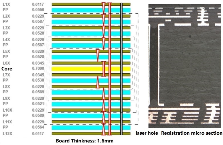
| Palo ea Lera | 4-60L |
| Fumaneha HDI PCB Technology | 1 + N + 1 |
| 2 + N + 2 | |
| 3 + N + 3 | |
| 4 + N + 4 | |
| 5 + N + 5 | |
| Lera lefe kapa lefe | |
| Botenya | 0.3mm-6mm |
| Bophara ba mola le Bonyane | 0.05mm / 0.05mm (2mil / 2mil) |
| BGA PITCH | 0.35 limilimithara |
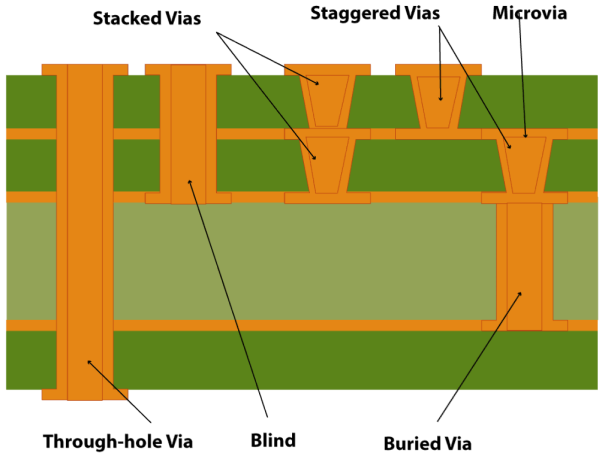
| Mets tham mong bang laser e ile ea fata Size | 0.075mm (3nil) |
| Mets phethahetse Drilled Size | 0.15mm (6mil) |
| Tekanyo ea likarolo tsa lesoba la laser | 0.9: 1 |
| Boemo ba tšobotsi bakeng sa lesoba | 16: 1 |
| Holim qeta | HASL, E etella pele mahala HASL, ENIG, qoelisoa Tin, OSP, qoelisoa Silver, Gold monoana, Electroplating Hard Khauta, khetla OSP , ENEPIG.etc. |
| Ka Khetho ea ho Tlatsa | Tsela e koahetsoe ebe e tlatsoa ka epoxy e tsamaisang kapa e sa tsamaeeng ebe e koaheloa ebe e koahetsoa |
| Koporo e tlatsitsoe, silevera e tletse | |
| Laser ka koporo tlotsitsoe koaloa | |
| Ngoliso | ± 4mil |
| Mask ea solder | Green, Red, Yellow, Blue, White, Black, Pherese, Matte Black, Matte tala.etc. |
Ithute haholoanyane ka lihlahisoa tsa YMS
Bala litaba tse ling


HDI PCB Manufacturing process
Products dihlopha
-

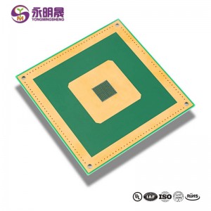
Micro ka PCB HDI PCB 8L 1 + N + 1 ka Via ka PAD | ETSANG
-

HDI PCB 2 + n + 2 VIPPO High kitlano Interconnect P ...
-

Wholesale Multi Layer PCB-PCB Manufacturer Chin...
-

HDI pcb 3 + N + 3 Laser ka koporo tlotsitsoe koaloa Cast ...
-

LED bontshiweng skrine pcb HDI tham mong bang laser ka ka PAD cop ...
-

HDI e hatisitsoeng liboto tsa potoloho 8Layer 2 Mohato HDI Bo ...


