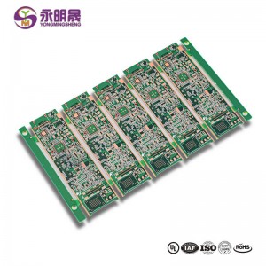
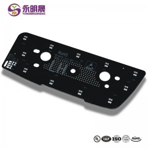
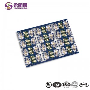
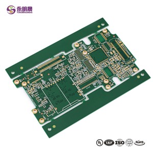
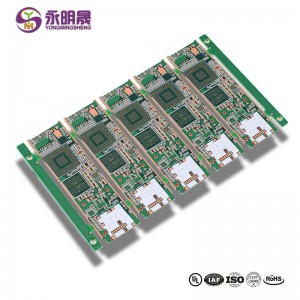
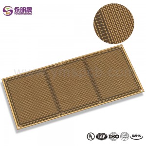
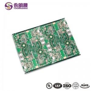
HDI PCB 12 Layer 2 Step HDI Board | YMS PCB
kwa
N'ígwé: 12
Base Material:FR4 High Tg EM827
Ọkpụrụkpụ : 1.2 ± 0.1mm
Min.Hole Size:0.15mm
Minimum Line Width/Space:0.075mm/0.075mm
Nwepu kacha nta n'etiti Layer Ne PTH na Line : 0.2mm
Size:101mm×55mm
Akụkụ ruru: 8: 1
N'elu omume: ENIG
Speciality: Laser via copper plated shut,VIPPO Technology,Blind Via and Buried Hole
Ngwa: Telecommunication
What is HDI PCBs?
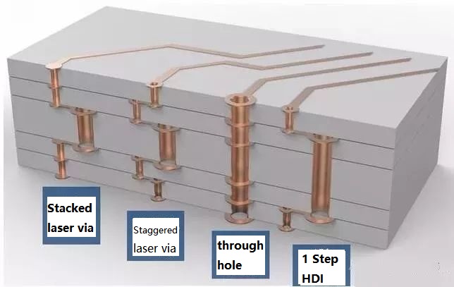
High density interconnect (HDI) PCBs represent one of the fastest-growing segments of the printed circuit board market. Because of its higher circuitry density, the HDI PCB design can incorporate finer lines and spaces, smaller vias and capture pads, and higher connection pad densities. A high-density PCB features blind and buried vias and often contains microvias that are .006 in diameter or even less.
1.Multi-nzọụkwụ HDI enyere njikọ dị n'etiti ọ bụla n'ígwé;
2.Cross-oyi akwa laser nhazi ike welie àgwà larịị nke multi-nzọụkwụ HDI;
3.The Nchikota HDI na elu ugboro ihe, metal dabeere laminates, FPC na ndị ọzọ pụrụ iche laminates na Filiks nwee mkpa nke elu njupụta na elu ugboro, elu okpomọkụ na-eduzi, ma ọ bụ 3D mgbakọ.
YMS HDI PCB n'ichepụta capa ọrụ:
| YMS HDI PCB n'ichepụta ike nnyocha | |
| Njirimara | ikike |
| Layer agụ | 4-60L |
| Nwere HDI PCB Technology | 1 + N + 1 |
| 2 + N + 2 | |
| 3 + N + 3 | |
| 4 + N + 4 | |
| 5 + N + 5 | |
| Ọ bụla oyi akwa | |
| Ọkpụrụkpụ | 0.3mm-6mm |
| Opekempe akara Obosara na Ohere | 0.05mm / 0.05mm (2mil / 2mil) |
| BGA PITCH | 0.35mm |
| Min laser gbapuru Size | 0.075mm (3nil) |
| Min n'ibu gbapuru Size | 0.15mm (6mil) |
| Akụkụ ruru maka laser onu | 0.9: 1 |
| Akụkụ Ratio maka site na oghere | 16: 1 |
| Elu rụchaa | HASL, Duru free HASL, ENIG, Imikpu Tin, OSP, ọlaọcha imikpu, mkpịsị aka mkpịsị aka, Ntinye ọla edo siri ike, ịhọrọ OSP , ENEPIG.etc. |
| Via Dejupụta Nhọrọ | The via na-plated ma jupụta ma conductive ma ọ bụ ndị na-abụghị conductive epoxy ahụ capped na plated |
| Ọla kọpa jupụtara, ọlaọcha jupụtara | |
| Laser site na ọla kọpa plated mechie | |
| Ndebanye aha | ± 4mil |
| Nkpuchi Solder | Green, Red, Yellow, Blue, White, Nwa, Purple, Matte Black, Matte green. Wdg. |
May nwere ike amasị:
1. The application range and circuit advantage of HDI board are introduced
2, PCB production skills: HDI board CAM production method
3, PCB design of 1 step, 2 step and 3step HDI


What is HDI in PCB?
HDI Boards – High Density Interconnect
What are the layers of a PCB?
Substrate Layer.
Copper Layer.
Soldermask layer.
Silkscreen layer.
What is HDI stackup?
HDI is short for high density interconnect, and refers to the use of buried, blind and micro vias as well as any layer HDIs to create compact boards.

