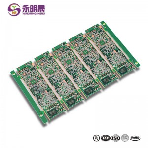
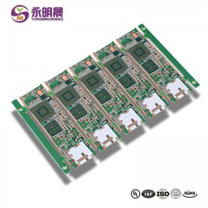
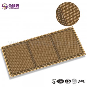
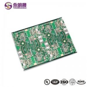
HDI PCB 12 Layer 2 Step HDI Board | YMS PCB
sile
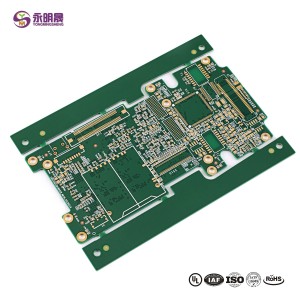
Fẹlẹfẹlẹ: 12
Base Material:FR4 High Tg EM827
Sisanra : 1.2 ± 0.1mm
Min.Hole Size:0.15mm
Minimum Line Width/Space:0.075mm/0.075mm
Iyatọ Kere laarin Layer Inner PTH ati Laini : 0.2mm
Size:101mm×55mm
Aspect ratio: 8: 1
Dada itọju: ENIG
Speciality: Laser via copper plated shut,VIPPO Technology,Blind Via and Buried Hole
Ohun elo: Telecommunication
What is HDI PCBs?
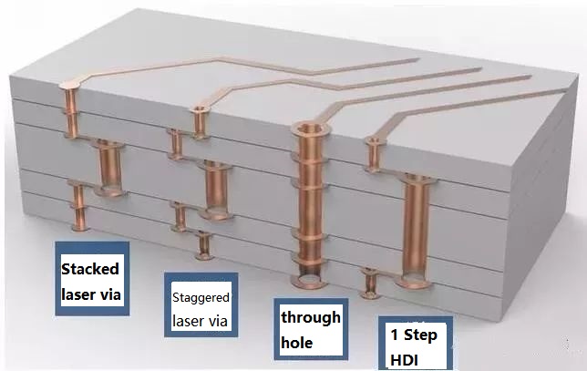
High density interconnect (HDI) PCBs represent one of the fastest-growing segments of the printed circuit board market. Because of its higher circuitry density, the HDI PCB design can incorporate finer lines and spaces, smaller vias and capture pads, and higher connection pad densities. A high-density PCB features blind and buried vias and often contains microvias that are .006 in diameter or even less.
1.Multi-ni igbese HDI kí awọn asopọ laarin eyikeyi fẹlẹfẹlẹ;
2.Cross-Layer lesa processing le mu awọn didara ipele ti olona-igbese HDI;
3.The apapo ti HDI ati ki o ga-igbohunsafẹfẹ ohun elo, irin-orisun laminates, FPC ati awọn miiran pataki laminates ati awọn ilana jeki awọn aini ti ga iwuwo ati ki o ga igbohunsafẹfẹ, ga ooru ifọnọhan, tabi 3D ijọ.
YMS HDI PCB iṣelọpọ awọn agbara kapa:
| Akopọ awọn agbara iṣelọpọ ẹrọ YMS HDI PCB | |
| Ẹya | awọn agbara |
| Ika Layer | 4-60L |
| Imọ-ẹrọ PCB HDI ti o wa | 1 + N + 1 |
| 2 + N + 2 | |
| 3 + N + 3 | |
| 4 + N + 4 | |
| 5 + N + 5 | |
| Layer eyikeyi | |
| Sisanra | 0.3mm-6mm |
| Iwọn ati Iwọn ila kekere | 0.05mm / 0.05mm (2mil / 2mil) |
| BGA Agbo | 0.35mm |
| Min lesa ti gbẹ iho Iwon | 0.075mm (3nil) |
| Min darí ti gbẹ iho Iwon | 0.15mm (6mil) |
| Ipele ipin fun iho lesa | 0.9: 1 |
| Ipele Ipele fun nipasẹ iho | 16: 1 |
| Ipari dada | HASL, Ṣiṣakoso HASL, ENIG, Tin immersion, OSP, Fadaka Imimimọ, Ika Goolu, Itanna Gold Giladi, Aṣayan OSP , ENEPIG.etc. |
| Nipasẹ Kun Aṣayan | O ti wa ni palara ati ki o kun pẹlu boya ifọnọhan tabi iposii ti ko ni ifọnọhan lẹhinna tan ati ki o fi sii |
| Ejò kun, fadaka kun | |
| Lesa nipasẹ idẹ ti pa | |
| Iforukọsilẹ | M 4mil |
| Boju Solder | Green, Red, Yellow, Blue, White, Black, Purple, Black Matte, Matte green.etc. |
O le Like:
1, The application range and circuit advantage of HDI board are introduced
2, PCB production skills: HDI board CAM production method
3, PCB design of 1 step, 2 step and 3step HDI
Kọ ẹkọ diẹ sii nipa awọn ọja YMS


What is HDI in PCB?
HDI Boards – High Density Interconnect
What are the layers of a PCB?
Substrate Layer.
Copper Layer.
Soldermask layer.
Silkscreen layer.
What is HDI stackup?
HDI is short for high density interconnect, and refers to the use of buried, blind and micro vias as well as any layer HDIs to create compact boards.

