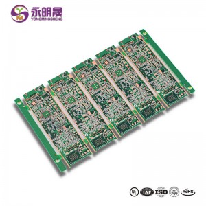
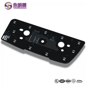
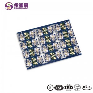
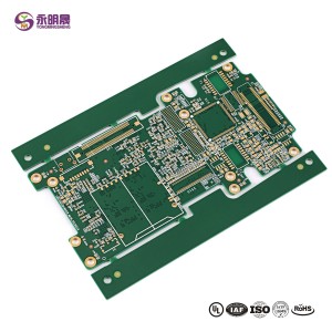
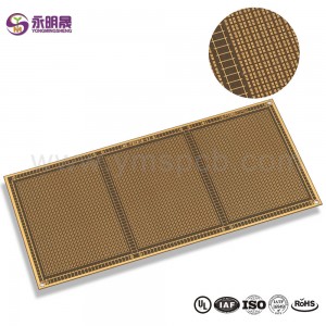
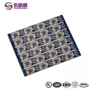
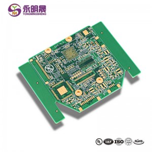
HDI PCB 12 Layer 2 Step HDI Board | YMS PCB
tawhā
Apa: 12
Base Material:FR4 High Tg EM827
Matotoru: 1.2 ± 0.1mm
Min.Hole Size:0.15mm
Minimum Line Width/Space:0.075mm/0.075mm
Te Maamaa Iti i waenga i te Apa o Roto PTH me te Raina : 0.2mm
Size:101mm×55mm
Aronga Ratio: 8: 1
maimoatanga Mata: ENIG
Speciality: Laser via copper plated shut,VIPPO Technology,Blind Via and Buried Hole
Tono: Telecommunication
What is HDI PCBs?
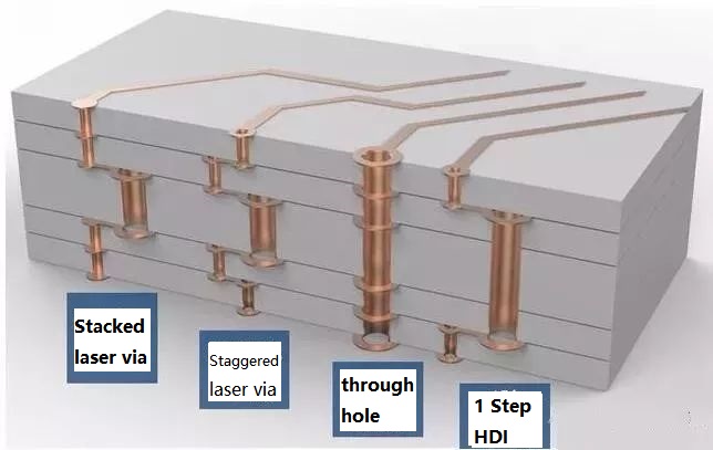
High density interconnect (HDI) PCBs represent one of the fastest-growing segments of the printed circuit board market. Because of its higher circuitry density, the Ko te HDI PCB design can incorporate finer lines and spaces, smaller vias and capture pads, and higher connection pad densities. A high-density PCB features blind and buried vias and often contains microvias that are .006 in diameter or even less.
1.Multi-step HDI āhei te hononga i waenganui i tetahi papa;
Ka taea e 2.Cross-apa tukatuka taiaho whakarei i te taumata kounga o maha-step HDI;
3.The huinga o HDI me ngā rauemi tiketike-auau, laminates hāngai whakarewa-, FPC me ētahi atu laminates motuhake me ngā tukanga taea nga hiahia o te kiato nui, me te auau tiketike, whakahaerenga wera tiketike, ranei huihui 3D.
YMS HDI PCB whakahoahoa i nga hononga capa :
| YMS HDI PCB whakangao tirohanga kaha | |
| Āhuahira | āheinga |
| Kaute Papa | 4-60L |
| Kei te waatea HDI PCB Hangarau | 1 + N + 1 |
| 2 + N + 2 | |
| 3 + N + 3 | |
| 4 + N + 4 | |
| 5 + N + 5 | |
| Tetahi paparanga | |
| Matotoru | 0.3mm-6mm |
| Raina Itinga Whanui me te Mokowā | 0.05mm / 0.05mm (2mil / 2mil) |
| BGA PITCH | 0.35mm |
| Min laser Te Rahi Rore | 0.075mm (3nil) |
| Te miihini Min | 0.15mm (6mil) |
| Ratio Wahanga mo te poka laser | 0.9: 1 |
| Ratio Wahanga mo te poka | 16: 1 |
| Mata Whakamutunga | HASL, Lead free HASL, ENIG, Immersion Tin, OSP, Immersion Silver, Gold Finger, Electroplating Hard Gold, Selective OSP, ENEPIG.etc. |
| Ma te Kii Whakakii | Ka whakakikihia te via ka whakakiihia ki te epoxy arataki kore-arataki ranei ka kapi ka pani |
| Kapi kapi, kapi hiriwa | |
| Taiaho ma te parahi whakakikoruatia tutakina | |
| Rehitatanga | ± 4mira |
| Mask Topi | Kakarariki, Whero, kowhai, Kahurangi, Ma, Mangu, Waiporoporo, Matte Pango, Matte matariki. |
Akene Ka Pai koe:
1, The application range and circuit advantage of HDI board are introduced
2, PCB production skills: HDI board CAM production method
3, PCB design of 1 step, 2 step and 3step HDI


What is HDI in PCB?
HDI Boards – High Density Interconnect
What are the layers of a PCB?
Substrate Layer.
Copper Layer.
Soldermask layer.
Silkscreen layer.
What is HDI stackup?
HDI is short for high density interconnect, and refers to the use of buried, blind and micro vias as well as any layer HDIs to create compact boards.

