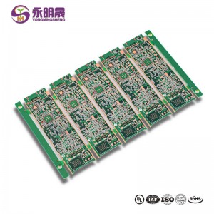
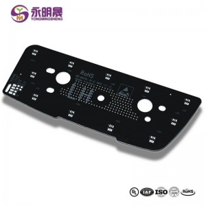
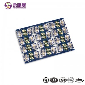
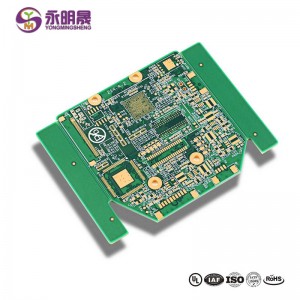
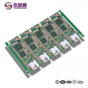
HDI PCB 12 Layer 2 Step HDI Board | YMS PCB
Morbi
Stratis: XII
Base Material:FR4 High Tg EM827
Crassitudine: 0.1mm ± 1,2
Min.Hole Size:0.15mm
Minimum Line Width/Space:0.075mm/0.075mm
Iacuit inter interiorem et linea PTH minimum Clearance: 0.2mm
Size:101mm×55mm
Aspect Ratio: VIII: I
Superficiem treatment: enig
Speciality: Laser via copper plated shut,VIPPO Technology,Blind Via and Buried Hole
Applications: Telecommunication
What is HDI PCBs?
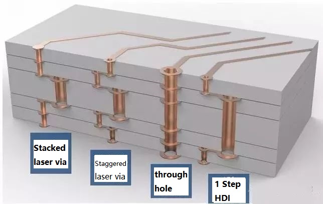
High density interconnect (HDI) PCBs represent one of the fastest-growing segments of the printed circuit board market. Because of its higher circuitry density, the PCB HDI design can incorporate finer lines and spaces, smaller vias and capture pads, and higher connection pad densities. A high-density PCB features blind and buried vias and often contains microvias that are .006 in diameter or even less.
1.Multi HDI-gradus ope nexum aliquem inter ordines,
2.Cross laser capillus-algarum multi-step processus potest augendae quale planum est HDI:
3. Et concursus istorum HDI summus frequency materiae, secundum metallum, laminates, FPC et alias speciales necessitates de laminates et processus ad enable excelsum densitate et frequency altum, altum calor ductu, vel 3D ecclesiam.
YMS HDI PCB faciens capa capacitatem capam;
| YMS HDI PCB vestibulum elit Overview | |
| feature | facultatem |
| stratum comitis | 4-60L |
| Available HDI PCB Technology | I + I + N |
| II + + N II | |
| III III + + N | |
| IV + + N IV | |
| V + + N V | |
| accumsan nec | |
| crassitudine | 0.3mm-6mm |
| Vivamus ipsum aciem spatium minimum | 0.05mm / 0.05mm (2mil / 2mil) |
| BGA CASTRA | 0.35mm |
| Min Location laser capillus Drilled | 0.075mm (3nil) |
| Min Location mechanica Drilled | 0.15mm (6mil) |
| Aspect laser ratio foraminis | 0,9: I |
| Aspect Ratio enim per foraminis | XVI: I |
| Conclusio superficiem | Removerit, removerit Category: enig, immersionis Stannum OSP immersionis argenti Digitus Aurum, Aurum Puer electroplating, electionem selectivam OSP ENEPIG.etc. |
| Via Bene Reple | Et per hoc in patella repleti PROLIXUS vel epoxy erit PROLIXUS vel non-capped et super patella |
| Aere impleta implebitur pecunia | |
| Laser aeris patella per operculi | |
| Registration | ± 4mil |
| Os solidaturam | Viridis, Red, Yellow, cæruleus, albus, Nigrum, Purple, Matte Nigrum, Matte green.etc. |
Sit Amo te:
1 The application range and circuit advantage of HDI board are introduced
2. PCB production skills: HDI board CAM production method
3、PCB design of 1 step, 2 step and 3step HDI


What is HDI in PCB?
HDI Boards – High Density Interconnect
What are the layers of a PCB?
Substrate Layer.
Copper Layer.
Soldermask layer.
Silkscreen layer.
What is HDI stackup?
HDI is short for high density interconnect, and refers to the use of buried, blind and micro vias as well as any layer HDIs to create compact boards.

